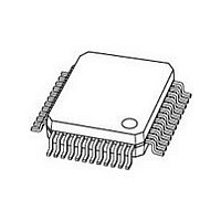
SC16C2550IB48,128 NXP Semiconductors, SC16C2550IB48,128 Datasheet - Page 13

SC16C2550IB48,128
Manufacturer Part Number
SC16C2550IB48,128
Description
IC DUART SOT313-2
Manufacturer
NXP Semiconductors
Datasheet
1.SC16C2550IN40112.pdf
(46 pages)
Specifications of SC16C2550IB48,128
Features
2 Channels
Number Of Channels
2, DUART
Fifo's
16 Byte
Voltage - Supply
3.5 V ~ 4.5 V
With Auto Flow Control
Yes
With Irda Encoder/decoder
Yes
With False Start Bit Detection
Yes
With Modem Control
Yes
With Cmos
Yes
Mounting Type
Surface Mount
Package / Case
48-LQFP
Transmit Fifo
16Byte
Receive Fifo
16Byte
Transmitter And Receiver Fifo Counter
Yes
Data Rate
5Mbps
Package Type
LQFP
Operating Supply Voltage (max)
5.5V
Mounting
Surface Mount
Pin Count
48
Operating Temperature (min)
-40C
Operating Temperature (max)
85C
Operating Temperature Classification
Industrial
Lead Free Status / RoHS Status
Lead free / RoHS Compliant
Other names
935270020128
SC16C2550IB48-T
SC16C2550IB48-T
SC16C2550IB48-T
SC16C2550IB48-T
Philips Semiconductors
9397 750 11621
Product data
6.8 Programmable baud rate generator
receive holding register (RHR) is read. The actual time-out value is 4 character time,
including data information length, start bit, parity bit, and the size of stop bit, i.e., 1 ,
1.5 , or 2 bit times.
The SC16C2550 supports high speed modem technologies that have increased input
data rates by employing data compression schemes. For example, a 33.6 kbit/s
modem that employs data compression may require a 115.2 kbit/s input data rate.
A 128.0 kbit/s ISDN modem that supports data compression may need an input
data rate of 460.8 kbit/s. The SC16C2550 can support a standard data rate of
921.6 kbit/s.
A single baud rate generator is provided for the transmitter and receiver, allowing
independent TX/RX channel control. The programmable Baud Rate Generator is
capable of operating with a frequency of up to 80 MHz. To obtain maximum data rate,
it is necessary to use full rail swing on the clock input. The SC16C2550 can be
configured for internal or external clock operation. For internal clock oscillator
operation, an industry standard microprocessor crystal is connected externally
between the XTAL1 and XTAL2 pins. Alternatively, an external clock can be
connected to the XTAL1 pin to clock the internal baud rate generator for standard or
custom rates (see
The generator divides the input 16 clock by any divisor from 1 to 2
SC16C2550 divides the basic external clock by 16. The basic 16 clock provides
table rates to support standard and custom applications using the same system
design. The rate table is configured via the DLL and DLM internal register functions.
Customized Baud Rates can be achieved by selecting the proper divisor values for
the MSB and LSB sections of baud rate generator.
Programming the Baud Rate Generator Registers DLM (MSB) and DLL (LSB)
provides a user capability for selecting the desired final baud rate. The example in
Table 6
external clock input.
Fig 5. Crystal oscillator connection.
shows the selectable baud rate table available when using a 1.8432 MHz
Dual UART with 16 bytes of transmit and receive FIFOs and IrDA
Table
Rev. 03 — 19 June 2003
C1
47 pF
1.8432 MHz
X1
6).
C2
100 pF
1.8432 MHz
C1
22 pF
© Koninklijke Philips Electronics N.V. 2003. All rights reserved.
X1
SC16C2550
1.5 k
C2
47 pF
002aaa169
encoder/decoder
16
1. The
13 of 46


