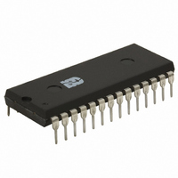
ISD5008PY Nuvoton Technology Corporation of America, ISD5008PY Datasheet - Page 26

ISD5008PY
Manufacturer Part Number
ISD5008PY
Description
IC VOICE REC/PLAY 4-8MIN 28-DIP
Manufacturer
Nuvoton Technology Corporation of America
Series
ISD5008r
Specifications of ISD5008PY
Interface
SPI/Microwire
Filter Pass Band
1.7 ~ 3.4kHz
Duration
4 ~ 8 Min
Mounting Type
Through Hole
Package / Case
28-DIP (0.600", 15.24mm)
For Use With
ISD-ES511 - EVALUATION SYSTEM FOR ISD5100ISD-ES501 - EVALUATION SYSTEM FOR ISD5008
Lead Free Status / RoHS Status
Lead free / RoHS Compliant
Available stocks
Company
Part Number
Manufacturer
Quantity
Price
Company:
Part Number:
ISD5008PY
Manufacturer:
Nuvoton
Quantity:
226
ISD5008 Product
To select this mode, the following control bits must
be configured in the ISD5008 configuration regis-
ters. To set up the transmit path:
To set up the receive path:
22
1. Select the FTHRU path through the ANA OUT
2. Power up the ANA OUT amplifier —Bit AOPD
1. Set up the ANA IN amplifier for the correct
2. Power up the ANA IN amplifier —Bit AIPD
3. Select the ANA IN path through the OUTPUT
4. Power up the Speaker Amplifier —Bits OPA0
MUX— Bits AOS0, AOS1 and AOS2 control
the state of the ANAOUT MUX. These are the
D6, D7 and D8 bits respectively of Configu-
ration Register 0 (CFG0) and they should all
be ZERO to select the FTHRU path.
controls the power up state of ANA OUT. This
is bit D5 of CFG0 and it should be a ZERO
to power up the amplifier.
gain —Bits AIG0 and AIG1 control the gain
settings of this amplifier. These are bits D14
and D15 respectively of CFG0. The input
level at this pin determines the setting of
this gain stage. Table 4 will help determine
this setting. In this example we will assume
that the peak signal never goes above 1
volt p-p single ended. That would enable
us to use the 9dB attenuation setting, or
where D14 is ONE and D15 is ZERO.
controls the power up state of ANA IN. This
is bit D13 of CFG0 and should be a ZERO to
power up the amplifier.
MUX —Bits OPS0 and OPS1 control the state
of the OUTPUT MUX. These are bits D3 and
D4 respectively of CFG0 and they should
be set to the state where D3 is ONE and D4
is ZERO to select the ANA IN path.
and OPA1 control the state of the Speaker
and AUX amplifiers. These are bits D1 and
D2 respectively of CFG0. They should be
set to the state where D1 is ONE and D2 is
ZERO. This powers up the Speaker Amplifier
and configures it for it’s higher gain setting
for use with a piezo speaker element and
also powers down the AUX output stage.
The status of the rest of the functions in the ISD5008
chip must be defined before the configuration
registers settings are updated:
1. Power down the Volume Control Ele-
2. Power down the AUX IN amplifier—Bit
3. Power down the SUM1 and SUM2 Mixer
4. Power down the FILTER stage—Bit FLPD
5. Power down the AGC amplifier—Bit
6. Don’t Care bits—The following stages are
ment—Bit VLPD controls the power up state
of the Volume Control. This is bit D0 of CFG0
and it should be set to a ONE to power
down this stage.
AXPD controls the power up state of the
AUX IN input amplifier. This is bit D10 of
CFG0 and it should be set to a ONE to pow-
er down this stage.
amplifiers—Bits S1M0 and S1M1 control
the SUM1 mixer and bits S2M0 and S2M1
control the SUM2 mixer. These are bits D7
and D8 in CFG1 and bits D5 and D6 in
CFG1 respectively. All 4 bits should be set
to a ONE to power down these two amplifi-
ers.
controls the power up state of the FILTER
stage in the device. This is bit D1 in CFG1
and should be set to a ONE to power down
the stage.
AGPD controls the power up state of the
AGC amplifier. This is bit D0 in CFG1 and
should be set to a ONE to power down this
stage.
not used in Feed Through Mode. Their bits
may be set to either level. In this example
we will set all the following bits to a ZERO.
(a). Bit INS0, bit D9 of CFG0 controls the In-
put Source Mux. (b). Bits AXG0 and AXG1
are bits D11 and D12 respectively in CFG0.
They control the AUX IN amplifier gain set-
ting. (c). Bits FLD0 and FLD1 are bits D2 and
D3 respectively in CFG1. They control the
sample rate and filter band pass setting.
(d). Bit FLS0 is bit D4 in CFG1. It controls the
FILTER MUX. (e). Bits S1S0 and S1S1 are bits
Voice Solutions in Silicon
™


