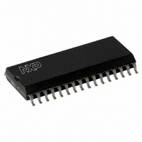
TDA8932BT/N2,112 NXP Semiconductors, TDA8932BT/N2,112 Datasheet - Page 16

TDA8932BT/N2,112
Manufacturer Part Number
TDA8932BT/N2,112
Description
IC AMP AUDIO 55W STER D 32SOIC
Manufacturer
NXP Semiconductors
Type
Class Dr
Datasheet
1.TDA8932BTWN2118.pdf
(48 pages)
Specifications of TDA8932BT/N2,112
Output Type
1-Channel (Mono) or 2-Channel (Stereo)
Package / Case
32-SOIC (7.5mm Width)
Max Output Power X Channels @ Load
55W x 1 @ 8 Ohm; 26.5W x 2 @ 4 Ohm
Voltage - Supply
10 V ~ 36 V, ±5 V ~ 18 V
Features
Depop, Differential Inputs, Mute, Short-Circuit and Thermal Protection
Mounting Type
Surface Mount
Product
Class-D
Output Power
55 W
Available Set Gain
36 dB
Common Mode Rejection Ratio (min)
75 dB
Thd Plus Noise
0.007 %
Operating Supply Voltage
22 V
Supply Current
145 mA
Maximum Power Dissipation
5000 mW
Maximum Operating Temperature
+ 85 C
Mounting Style
SMD/SMT
Audio Load Resistance
8 Ohms
Dual Supply Voltage
+/- 11 V
Input Signal Type
Differential
Minimum Operating Temperature
- 40 C
Output Signal Type
Differential, Single
Supply Type
Single or Dual
Supply Voltage (max)
36 V
Supply Voltage (min)
10 V
Lead Free Status / RoHS Status
Lead free / RoHS Compliant
Other names
935283477112
TDA8932BT
TDA8932BT
TDA8932BT
TDA8932BT
NXP Semiconductors
10. Limiting values
11. Thermal characteristics
Table 9.
TDA8932B_4
Product data sheet
Symbol
SO32 package
R
th(j-a)
j-lead
j-top
Thermal characteristics
Parameter
thermal resistance from junction
to ambient
thermal characterization
parameter from junction to lead
thermal characterization
parameter from junction to top of
package
Table 8.
In accordance with the Absolute Maximum Rating System (IEC 60134).
[1]
[2]
[3]
[4]
[5]
[6]
[7]
[8]
Symbol Parameter
V
V
I
T
T
T
P
V
ORM
j
stg
amb
P
x
esd
V
Measured with respect to pin INREF; V
Measured with respect to pin V
Measured with respect to pin CGND; V
V
Current limiting concept.
Human Body Model (HBM); R
For pins 2, 3, 11, 14 and 15 V
Machine Model (MM); R
P
SS
= V
= V
DDP1
supply voltage
voltage on pin x
repetitive peak output
current
junction temperature
storage temperature
ambient temperature
power dissipation
electrostatic discharge
voltage
SSP1
Limiting values
IN1P, IN1N, IN2P, IN2N
OSCREF, OSCIO, TEST
POWERUP, ENGAGE,
DIAG
all other pins
= V
V
SSP1
SSP2
= V
Conditions
free air natural convection
; V
Rev. 04 — 18 December 2008
JEDEC test board
2 layer application board
DD
DDP2
s
= 0 ; C = 200 pF; L = 0.75 H.
= V
esd
DDP1
s
V
SSD(HW)
= 1500 ; C = 100 pF
SSP2
= 1800 V.
= V
.
; V
DDP2
x
x
Conditions
asymmetrical supply
maximum output
current limiting
HBM
MM
< V
< V
x
< V
.
DD
DD
DD
+ 0.3 V.
+ 0.3 V.
+ 0.3 V.
[1]
[2]
[3]
[4]
[1]
[2]
[3]
[5]
[6]
[7]
[8]
Min
-
-
-
-
Min
V
V
V
4
-
-
0.3
5
55
40
2000
200
SSD(HW)
CGND
SS
Class-D audio amplifier
0.3
Typ
41
44
-
-
TDA8932B
0.3
0.3 5
© NXP B.V. 2008. All rights reserved.
Max
+40
+5
6
V
-
150
+150
+85
5
+2000
+200
Max
44
-
30
8
DD
+ 0.3 V
16 of 48
Unit
K/W
K/W
K/W
K/W
Unit
V
V
V
V
A
W
V
V
C
C
C


