TFA9800J/N1,112 NXP Semiconductors, TFA9800J/N1,112 Datasheet
TFA9800J/N1,112
Specifications of TFA9800J/N1,112
TFA9800J
TFA9800J


Related parts for TFA9800J/N1,112


TFA9800J/N1,112 Summary of contents
Page 1
TFA9800J 2 Rev. 01 — 17 March 2006 1. General description The TFA9800 is an integrated class-AB dual output amplifi 9-pin DIL-bent-SIL (DBS9P) power package. The device is primarily developed for CRT and multi-media applications. 2. Features Requires ...
Page 2
Philips Semiconductors Table 1: Symbol Parameter n(o)(rms [1] The circuit is DC adjusted at V [2] Output power is measured directly at the output pins of the TFA9800J. 4. Ordering information Table 2: Type number ...
Page 3
Philips Semiconductors 5. Block diagram non-inverting supply voltage ripple rejection non-inverting Fig 1. Block diagram TFA9800J_1 Preliminary data sheet 1 mute switch input stand-by switch output 18 ...
Page 4
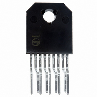
Philips Semiconductors 6. Pinning information 6.1 Pinning Fig 2. Pin configuration SOT523-1 6.2 Pin description Table 3: Symbol INV1 SGND SVRR OUT1 PGND OUT2 V P M/SS INV2 7. Functional description The TFA9800J contains two identical amplifiers with differential input ...
Page 5
Philips Semiconductors 8. Limiting values Table 4: In accordance with the Absolute Maximum Rating System (IEC 60134). Symbol P(sc) V P(r) E hand(O) I OSM I ORM P tot T stg T amb T j [1] The ...
Page 6
Philips Semiconductors Table 6: Symbol V th(on) V th(mute) V th(stb) [1] The circuit is DC adjusted at V 11. Dynamic characteristics Table Symbol P o THD f -3db(l) f -1db( ...
Page 7
Philips Semiconductors 12. Application information 12.1 Printed-Circuit Board (PCB) layout and grounding For high system performance level, certain grounding techniques are imperative. The input reference grounds have to be tied with their respective source grounds and must have separate traces ...
Page 8
Philips Semiconductors 12.4 Output power The output power versus supply voltage has been measured on the output pins and at THD = 10 %. The maximum output power is limited by the maximum allowable power dissipation and the maximum available ...
Page 9
Philips Semiconductors slow. Unfortunately, the slope of the SVRR voltage is not well controlled in the phase where the SVRR voltage is between ground and ground + 0 other words SVRR makes a step and so does the ...
Page 10
Philips Semiconductors mute 4.7 F BC337 anti plop 200 k BAW62 200 k anti plop 1 Fig 4. Implementation diagram for plop improvement a. Bottom side Fig 5. Printed-circuit board copper ...
Page 11
Philips Semiconductors Fig 6. Printed-circuit board component layout for single-ended application 12.11 Typical performance characteristics for single-ended application The test conditions, unless otherwise specified, are single-ended stereo application; fixed gain equals 20 dB; audio band ...
Page 12
Philips Semiconductors 0 SVRR (dB 100 Fig 9. Supply voltage ripple rejection as a function of frequency 10 P tot ( ...
Page 13
Philips Semiconductors 13. Package outline DBS9P: plastic DIL-bent-SIL power package; 9 leads (lead length 12/11 mm); exposed die pad DIMENSIONS (mm are the original dimensions) (2) (1) (2) UNIT ...
Page 14
Philips Semiconductors 14. Soldering 14.1 Introduction to soldering through-hole mount packages This text gives a brief insight to wave, dip and manual soldering. A more in-depth account of soldering ICs can be found in our Data Handbook IC26; Integrated Circuit ...
Page 15
Philips Semiconductors 15. Revision history Table 10: Revision history Document ID Release date TFA9800J_1 20060317 TFA9800J_1 Preliminary data sheet Data sheet status Change notice Preliminary data sheet - Rev. 01 — 17 March 2006 TFA9800J stereo power ...
Page 16
Philips Semiconductors 16. Data sheet status [1] Level Data sheet status Product status I Objective data Development II Preliminary data Qualification III Product data Production [1] Please consult the most recently issued data sheet before initiating or completing a design. ...
Page 17
Philips Semiconductors 21. Contents 1 General description . . . . . . . . . . . . . . . . . . . . . . 1 2 Features . . . . . . . . ...