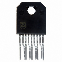
TFA9800J/N1,112 NXP Semiconductors, TFA9800J/N1,112 Datasheet - Page 9

TFA9800J/N1,112
Manufacturer Part Number
TFA9800J/N1,112
Description
IC AMP AUDIO PWR 7W STER AB 9SIL
Manufacturer
NXP Semiconductors
Type
Class ABr
Datasheet
1.TFA9800JN1112.pdf
(17 pages)
Specifications of TFA9800J/N1,112
Output Type
2-Channel (Stereo)
Package / Case
9-SIL (Bent and Staggered Leads)
Max Output Power X Channels @ Load
7W x 2 @ 4 Ohm
Voltage - Supply
6 V ~ 18 V
Features
Depop, Mute, Short-Circuit and Thermal Protection, Standby
Mounting Type
Through Hole
Product
Class-AB
Output Power
7 W
Available Set Gain
20 dB
Thd Plus Noise
0.1 %
Operating Supply Voltage
15 V
Supply Current
40 mA
Maximum Power Dissipation
25 W
Maximum Operating Temperature
+ 85 C
Mounting Style
Through Hole
Audio Load Resistance
4 Ohms
Input Signal Type
Differential
Minimum Operating Temperature
- 40 C
Output Signal Type
Single
Supply Type
Single
Supply Voltage (max)
18 V
Supply Voltage (min)
6 V
Lead Free Status / RoHS Status
Lead free / RoHS Compliant
Other names
935279697112
TFA9800J
TFA9800J
TFA9800J
TFA9800J
Philips Semiconductors
TFA9800J_1
Preliminary data sheet
12.10 Application diagram and board layout
12.9 Thermal behavior
slow. Unfortunately, the slope of the SVRR voltage is not well controlled in the phase
where the SVRR voltage is between ground and ground + 0.7 V. In other words SVRR
makes a step and so does the output. Consequently a plop sound can occur.
Solution is to give the SVRR pin a bias, see anti plop 1 in
is to give the DC-outputs of the load a bias, see anti plop 2
The turn-on and turn-off time can be influenced by an RC-circuit on the pin M/SS; see anti
plop 3 in
plop noise. A proper timing on pin M/SS can prevent this; see
The typical thermal resistance of the TFA9800J in the DBS9P package (R
The thermal resistance (R
22 cm
calculation can be made for the application at V
power dissipation is about 4 W:
Remark: The calculation holds for applications at average listening level music output
signals. Applying or testing with sine wave signals will produce about 1.5
power dissipation. At worst-case condition this can activate the maximum temperature
protection.
The single-ended application circuit diagram is shown in
application is shown in
T
Fig 3. Single-ended application block diagram
j max
2
is about 16 K/W. For a maximum ambient temperature of 60 C the following
=
Figure
T
amb
+
4. Rapid on/off switching of the device or pin M/SS may cause click and
IN1
IN2
P
tot
220 nF
220 nF
Rev. 01 — 17 March 2006
Figure 5
R
th j c
th(h-a)
INV1
INV2
–
1
9
) of an aluminium heat-sink with a (one-side) area of about
+
and
R
SGND
th h a
Figure
8
TFA9800J
2
–
6.
PGND
V
ref
7
T
5
P
j max
= 15 V, R
4
3
6
=
OUT1
SVRR
OUT2
60
Figure
Figure
2
+
© Koninklijke Philips Electronics N.V. 2006. All rights reserved.
L
Figure
100
100
= 4
4.0
nF
7 W stereo power amplifier
F
Figure
3. The PCB layout for this
4. A second improvement
001aad580
4.
1000
1000
and the ALL music
4
2200
F
4
F
4
F
+
TFA9800J
4.
16
V
P
th(j-c)
=
the music
140 C
) is 4 K/W.
9 of 17


