TFA9800J/N1,112 NXP Semiconductors, TFA9800J/N1,112 Datasheet - Page 8
TFA9800J/N1,112
Manufacturer Part Number
TFA9800J/N1,112
Description
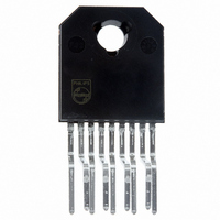
IC AMP AUDIO PWR 7W STER AB 9SIL
Manufacturer
NXP Semiconductors
Type
Class ABr
Datasheet
1.TFA9800JN1112.pdf
(17 pages)
Specifications of TFA9800J/N1,112
Output Type
2-Channel (Stereo)
Package / Case
9-SIL (Bent and Staggered Leads)
Max Output Power X Channels @ Load
7W x 2 @ 4 Ohm
Voltage - Supply
6 V ~ 18 V
Features
Depop, Mute, Short-Circuit and Thermal Protection, Standby
Mounting Type
Through Hole
Product
Class-AB
Output Power
7 W
Available Set Gain
20 dB
Thd Plus Noise
0.1 %
Operating Supply Voltage
15 V
Supply Current
40 mA
Maximum Power Dissipation
25 W
Maximum Operating Temperature
+ 85 C
Mounting Style
Through Hole
Audio Load Resistance
4 Ohms
Input Signal Type
Differential
Minimum Operating Temperature
- 40 C
Output Signal Type
Single
Supply Type
Single
Supply Voltage (max)
18 V
Supply Voltage (min)
6 V
Lead Free Status / RoHS Status
Lead free / RoHS Compliant
Other names
935279697112
TFA9800J
TFA9800J
TFA9800J
TFA9800J


Philips Semiconductors
TFA9800J_1
Preliminary data sheet
12.4 Output power
12.5 Supply voltage ripple rejection
12.6 Headroom
12.7 Pin M/SS
12.8 Switch on and switch off
The output power versus supply voltage has been measured on the output pins and at
THD = 10 %. The maximum output power is limited by the maximum allowable power
dissipation and the maximum available output current: 2.5 A repetitive peak current; see
Figure
The SVRR has been measured with an electrolytic capacitor of 100 F on pin 3 and at a
bandwidth of 10 Hz to 80 kHz. Both curves for operating and mute condition were
measured with R
A typical music CD requires at least 12 dB (= factor 15.85) dynamic headroom compared
with the average power output for passing the loudest portions without distortion. The
following calculation can be made for this application at V
P
any distortion yields: P
can be derived for a headroom of 0 dB and 12 dB respectively:
Table 8:
So for average listening level music power, a power dissipation of 4 W can be used for the
thermal behavior calculation as described in
For the three functional modes: Standby mode, Mute mode, and Operating mode, pin
M/SS can be driven by a 3-state logic output stage, e.g. microcontroller with some extra
components for DC-level shifting; see
To avoid audible plops during switch on or switch off of the supply voltage, pin M/SS has to
be set in Standby condition (GND level) before the voltage is applied (switch-on) or
removed (switch-off). Via the Mute mode the input- and SVRR-capacitors are smoothly
charged (or discharged). The slope of the SVRR-voltage should be well controlled and
Condition
P
o
•
•
•
o
at THD = 0.2 % is about 4.5 W; see
= 4.5 W at THD = 0.2 %
Standby mode is activated by a low DC level, between 0 V and 2 V on pin M/SS. The
power consumption of the TFA9800J will be reduced to < 0.1 mW
Mute mode will be activated by a DC level between 3.3 V and 6.4 V. The outputs of
the amplifier will be muted (no audio output), however the amplifier is DC biased and
the DC level of the output pins remains on half the supply voltage. The input coupling
capacitors are charged when in Mute mode to avoid plop noise.
The TFA9800J will be in Operating mode at pin M/SS voltages between 8.5 V and V
13.
Power rating
S
= 25 ; see
o
Rev. 01 — 17 March 2006
= 4.5 W / 15.85 = 284 mW. From
Headroom
0 dB
12 dB
Figure
Figure 10
9.
Figure
Section 12.9 “Thermal
7. Average Listening Level (ALL) without
for the respective DC levels.
2
Figure
P
© Koninklijke Philips Electronics N.V. 2006. All rights reserved.
= 15 V and R
Power dissipation
6 W
4 W
7 W stereo power amplifier
11, the power dissipation
behavior”.
TFA9800J
L
= 4 :
8 of 17
P
Related parts for TFA9800J/N1,112
Image
Part Number
Description
Manufacturer
Datasheet
Request
R

Part Number:
Description:
Tfa9800j 2 X 7 W Stereo Power Amplifier
Manufacturer:
NXP Semiconductors
Datasheet:

Part Number:
Description:
Audio Amplifiers 2X6W AUDIO AMPLIFIER
Manufacturer:
NXP Semiconductors
Datasheet:
Part Number:
Description:
NXP Semiconductors designed the LPC2420/2460 microcontroller around a 16-bit/32-bitARM7TDMI-S CPU core with real-time debug interfaces that include both JTAG andembedded trace
Manufacturer:
NXP Semiconductors
Datasheet:

Part Number:
Description:
NXP Semiconductors designed the LPC2458 microcontroller around a 16-bit/32-bitARM7TDMI-S CPU core with real-time debug interfaces that include both JTAG andembedded trace
Manufacturer:
NXP Semiconductors
Datasheet:
Part Number:
Description:
NXP Semiconductors designed the LPC2468 microcontroller around a 16-bit/32-bitARM7TDMI-S CPU core with real-time debug interfaces that include both JTAG andembedded trace
Manufacturer:
NXP Semiconductors
Datasheet:
Part Number:
Description:
NXP Semiconductors designed the LPC2470 microcontroller, powered by theARM7TDMI-S core, to be a highly integrated microcontroller for a wide range ofapplications that require advanced communications and high quality graphic displays
Manufacturer:
NXP Semiconductors
Datasheet:
Part Number:
Description:
NXP Semiconductors designed the LPC2478 microcontroller, powered by theARM7TDMI-S core, to be a highly integrated microcontroller for a wide range ofapplications that require advanced communications and high quality graphic displays
Manufacturer:
NXP Semiconductors
Datasheet:
Part Number:
Description:
The Philips Semiconductors XA (eXtended Architecture) family of 16-bit single-chip microcontrollers is powerful enough to easily handle the requirements of high performance embedded applications, yet inexpensive enough to compete in the market for hi
Manufacturer:
NXP Semiconductors
Datasheet:
Part Number:
Description:
The XA-S3 device is a member of Philips Semiconductors? XA(eXtended Architecture) family of high performance 16-bitsingle-chip microcontrollers
Manufacturer:
NXP Semiconductors
Datasheet:

Part Number:
Description:
The NXP BlueStreak LH75401/LH75411 family consists of two low-cost 16/32-bit System-on-Chip (SoC) devices
Manufacturer:
NXP Semiconductors
Datasheet:
Part Number:
Description:
The NXP LPC3130/3131 combine an 180 MHz ARM926EJ-S CPU core, high-speed USB2
Manufacturer:
NXP Semiconductors
Datasheet:
Part Number:
Description:
The NXP LPC3141 combine a 270 MHz ARM926EJ-S CPU core, High-speed USB 2
Manufacturer:
NXP Semiconductors
Part Number:
Description:
The NXP LPC3143 combine a 270 MHz ARM926EJ-S CPU core, High-speed USB 2
Manufacturer:
NXP Semiconductors

Part Number:
Description:
The NXP LPC3152 combines an 180 MHz ARM926EJ-S CPU core, High-speed USB 2
Manufacturer:
NXP Semiconductors