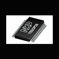
LPC1112FDH28 NXP Semiconductors, LPC1112FDH28 Datasheet - Page 42

LPC1112FDH28
Manufacturer Part Number
LPC1112FDH28
Description
The LPC1112FDH28 is an ARM Cortex-M0 based, low-cost 32-bit MCU, designed for 8/16-bit microcontroller applications, offering performance, low power, simple instruction set and memory addressing together with reduced code size compared to existing 8/
Manufacturer
NXP Semiconductors
Datasheet
1.LPC1110FD20.pdf
(103 pages)
Available stocks
Company
Part Number
Manufacturer
Quantity
Price
Part Number:
LPC1112FDH28
Manufacturer:
TI/德州仪器
Quantity:
20 000
Part Number:
LPC1112FDH28/102:5
Manufacturer:
NXP/恩智浦
Quantity:
20 000
NXP Semiconductors
LPC111X
Product data sheet
7.5.2 Interrupt sources
7.7.1 Features
7.6 IOCONFIG block
7.7 Fast general purpose parallel I/O
Each peripheral device has one interrupt line connected to the NVIC but may have several
interrupt flags. Individual interrupt flags may also represent more than one interrupt
source.
Any GPIO pin (total of up to 42 pins) regardless of the selected function, can be
programmed to generate an interrupt on a level, or rising edge or falling edge, or both.
The IOCONFIG block allows selected pins of the microcontroller to have more than one
function. Configuration registers control the multiplexers to allow connection between the
pin and the on-chip peripherals.
Peripherals should be connected to the appropriate pins prior to being activated and prior
to any related interrupt(s) being enabled. Activity of any enabled peripheral function that is
not mapped to a related pin should be considered undefined.
Device pins that are not connected to a specific peripheral function are controlled by the
GPIO registers. Pins may be dynamically configured as inputs or outputs. Multiple outputs
can be set or cleared in one write operation.
LPC1110/11/12/13/14/15 use accelerated GPIO functions:
Additionally, any GPIO pin (total of up to 42 pins) providing a digital function can be
programmed to generate an interrupt on a level, a rising or falling edge, or both.
•
•
•
•
•
•
•
•
•
•
In the LPC1110/11/12/13/14/15, the NVIC supports 32 vectored interrupts including up
to 13 inputs to the start logic from individual GPIO pins.
Four programmable interrupt priority levels with hardware priority level masking.
Software interrupt generation.
GPIO registers are a dedicated AHB peripheral so that the fastest possible I/O timing
can be achieved.
Entire port value can be written in one instruction.
Bit level port registers allow a single instruction to set or clear any number of bits in
one write operation.
Direction control of individual bits.
All I/O default to inputs with pull-ups enabled after reset with the exception of the
I
Pull-up/pull-down resistor configuration can be programmed through the IOCONFIG
block for each GPIO pin (except for pins PIO0_4 and PIO0_5).
On the LPC1100, all GPIO pins (except PIO0_4 and PIO0_5) are pulled up to 2.6 V
(V
2
C-bus pins PIO0_4 and PIO0_5.
DD
= 3.3 V) if their pull-up resistor is enabled in the IOCONFIG block.
All information provided in this document is subject to legal disclaimers.
Rev. 7 — 1 March 2012
LPC1110/11/12/13/14/15
32-bit ARM Cortex-M0 microcontroller
© NXP B.V. 2012. All rights reserved.
42 of 103


