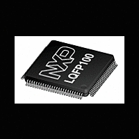
LPC2157_2158 NXP Semiconductors, LPC2157_2158 Datasheet - Page 25

LPC2157_2158
Manufacturer Part Number
LPC2157_2158
Description
The LPC2157/2158 is a multi-chip module consisting of a LPC2138/2148 single-chipmicrocontroller combined with a PCF8576D Universal LCD driver in a low-cost 100-pinpackage
Manufacturer
NXP Semiconductors
Datasheet
1.LPC2157_2158.pdf
(45 pages)
NXP Semiconductors
LPC2157_2158_2
Product data sheet
6.19.4 Brownout detector
6.19.5 Code security
6.19.6 External interrupt inputs
6.19.7 Memory mapping control
6.19.8 Power control
The LPC2157/2158 include 2-stage monitoring of the voltage on the V
voltage falls below 2.9 V, the BOD asserts an interrupt signal to the VIC. This signal can
be enabled for interrupt; if not, software can monitor the signal by reading dedicated
register.
The second stage of low voltage detection asserts reset to inactivate the LPC2157/2158
when the voltage on the V
flash as operation of the various elements of the chip would otherwise become unreliable
due to low voltage. The BOD circuit maintains this reset down below 1 V, at which point
the POR circuitry maintains the overall reset.
Both the 2.9 V and 2.6 V thresholds include some hysteresis. In normal operation, this
hysteresis allows the 2.9 V detection to reliably interrupt, or a regularly-executed event
loop to sense the condition.
This feature of the LPC2157/2158 allow an application to control whether it can be
debugged or protected from observation.
If after reset on-chip bootloader detects a valid checksum in flash and reads 0x8765 4321
from address 0x1FC in flash, debugging will be disabled and thus the code in flash will be
protected from observation. Once debugging is disabled, it can be enabled only by
performing a full chip erase using the ISP.
The LPC2157/2158 include up to nine edge or level sensitive external interrupt inputs as
selectable pin functions. When the pins are combined, external events can be processed
as four independent interrupt signals. The external interrupt inputs can optionally be used
to wake-up the processor from Power-down mode.
Additionally capture input pins can also be used as external interrupts without the option
to wake the device up from Power-down mode.
The Memory Mapping Control alters the mapping of the interrupt vectors that appear
beginning at address 0x0000 0000. Vectors may be mapped to the bottom of the on-chip
flash memory, or to the on-chip static RAM. This allows code running in different memory
spaces to have control of the interrupts.
The LPC2157/2158 supports two reduced power modes: Idle mode and Power-down
mode.
In Idle mode, execution of instructions is suspended until either a reset or interrupt occurs.
Peripheral functions continue operation during Idle mode and may generate interrupts to
cause the processor to resume execution. Idle mode eliminates power used by the
processor itself, memory systems and related controllers, and internal buses.
Rev. 02 — 9 February 2009
DD
pins falls below 2.6 V. This reset prevents alteration of the
Single-chip 16-bit/32-bit microcontrollers
LPC2157/2158
DD
© NXP B.V. 2009. All rights reserved.
pins. If this
25 of 45


