LPC2157_2158 NXP Semiconductors, LPC2157_2158 Datasheet - Page 26

LPC2157_2158
Manufacturer Part Number
LPC2157_2158
Description
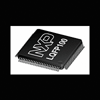
The LPC2157/2158 is a multi-chip module consisting of a LPC2138/2148 single-chipmicrocontroller combined with a PCF8576D Universal LCD driver in a low-cost 100-pinpackage
Manufacturer
NXP Semiconductors
Datasheet
1.LPC2157_2158.pdf
(45 pages)
NXP Semiconductors
LPC2157_2158_2
Product data sheet
6.19.9 APB bus
6.20.1 EmbeddedICE
6.20 Emulation and debugging
In Power-down mode, the oscillator is shut down and the chip receives no internal clocks.
The processor state and registers, peripheral registers, and internal SRAM values are
preserved throughout Power-down mode and the logic levels of chip output pins remain
static. The Power-down mode can be terminated and normal operation resumed by either
a reset or certain specific interrupts that are able to function without clocks. Since all
dynamic operation of the chip is suspended, Power-down mode reduces chip power
consumption to nearly zero.
Selecting an external 32 kHz clock instead of the PCLK as a clock-source for the on-chip
RTC will enable the microcontroller to have the RTC active during Power-down mode.
Power-down current is increased with RTC active. However, it is significantly lower than in
Idle mode.
A Power Control for Peripherals feature allows individual peripherals to be turned off if
they are not needed in the application, resulting in additional power savings during active
and Idle mode.
The APB divider determines the relationship between the processor clock (CCLK) and the
clock used by peripheral devices (PCLK). The APB divider serves two purposes. The first
is to provide peripherals with the desired PCLK via APB bus so that they can operate at
the speed chosen for the ARM processor. In order to achieve this, the APB bus may be
slowed down to
properly at power-up (and its timing cannot be altered if it does not work since the APB
divider control registers reside on the APB bus), the default condition at reset is for the
APB bus to run at
is to allow power savings when an application does not require any peripherals to run at
the full processor rate. Because the APB divider is connected to the PLL output, the PLL
remains active (if it was running) during Idle mode.
The LPC2157/2158 supports emulation and debugging via a JTAG serial port. Debugging
functions are multiplexed with GPIOs on Port 1. This means that all communication, timer
and interface peripherals residing on Port 0 are available during the development and
debugging phase as they are when the application is run in the embedded system itself.
Standard ARM EmbeddedICE logic provides on-chip debug support. The debugging of
the target system requires a host computer running the debugger software and an
EmbeddedICE protocol convertor. EmbeddedICE protocol convertor converts the remote
debug protocol commands to the JTAG data needed to access the ARM core.
The ARM core has a Debug Communications Channel (DCC) function built-in. The DCC
allows a program running on the target to communicate with the host debugger or another
separate host without stopping the program flow or even entering the debug state. The
DCC is accessed as a co-processor 14 by the program running on the ARM7TDMI-S
core. The DCC allows the JTAG port to be used for sending and receiving data without
affecting the normal program flow. The DCC data and control registers are mapped in to
addresses in the EmbeddedICE logic.
1
2
1
to
4
of the processor clock rate. The second purpose of the APB divider
1
Rev. 02 — 9 February 2009
4
of the processor clock rate. Because the APB bus must work
Single-chip 16-bit/32-bit microcontrollers
LPC2157/2158
© NXP B.V. 2009. All rights reserved.
26 of 45


