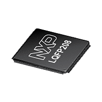
LPC2930 NXP Semiconductors, LPC2930 Datasheet - Page 29

LPC2930
Manufacturer Part Number
LPC2930
Description
The LPC2930 combine an ARM968E-S CPU core with two integrated TCM blocksoperating at frequencies of up to 125 MHz, Full-speed USB 2
Manufacturer
NXP Semiconductors
Datasheet
1.LPC2930.pdf
(98 pages)
Available stocks
Company
Part Number
Manufacturer
Quantity
Price
Company:
Part Number:
LPC2930FBD208
Manufacturer:
PHI
Quantity:
103
Company:
Part Number:
LPC2930FBD208,551
Manufacturer:
NXP Semiconductors
Quantity:
10 000
Company:
Part Number:
LPC2930FBD208551
Manufacturer:
NXP Semiconductors
Quantity:
135
Company:
Part Number:
LPC2930FET208,551
Manufacturer:
NXP Semiconductors
Quantity:
10 000
NXP Semiconductors
LPC2930_3
Product data sheet
6.10.4.1 Pin description
6.11.1 Peripheral subsystem clock description
6.11 Peripheral subsystem
The event router allows the event source to be defined, its polarity and activation type to
be selected and the interrupt to be masked or enabled. The event router can be used to
start a clock on an external event.
The vectored interrupt-controller inputs are active HIGH.
The event router module in the LPC2930 is connected to the pins listed below. The pins
are combined with other functions on the port pins of the LPC2930.
pins connected to the event router.
Table 14.
The peripheral subsystem is clocked by a number of different clocks:
Symbol
EXTINT[7:0]
CAN0 RXD
CAN1 RXD
I
I
LIN0 RXD
LIN1 RXD
SPI0 SDI
SPI1 SDI
SPI2 SDI
UART0 RXD
UART1 RXD
USB_SCL1
-
-
-
2
2
•
•
•
•
•
•
•
•
C0 SCL
C1 SCL
Programmable input level and edge polarity.
Event detection maskable.
Event detection is fully asynchronous, so no clock is required.
CLK_SYS_PESS
CLK_UART0/1
CLK_SPI0/1/2
CLK_TMR0/1/2/3
CLK_SAFE see
Event-router pin connections
All information provided in this document is subject to legal disclaimers.
Direction
I
I
I
I
I
I
I
I
I
I
I
I
I
na
na
na
Section 6.6.2
Rev. 03 — 16 April 2010
Description
external interrupt inputs 7 to 0
CAN0 receive data input wake-up
CAN1 receive data input wake-up
I
I
LIN0 receive data input wake-up
LIN1 receive data input wake-up
SPI0 receive data input
SPI1 receive data input
SPI2 receive data input
UART0 receive data input
UART1 receive data input
USB I
CAN interrupt (internal)
VIC FIQ (internal)
VIC IRQ (internal)
2
2
C0 SCL clock input
C1 SCL clock input
2
ARM9 microcontroller with CAN, LIN, and USB
C serial clock
Table 14
LPC2930
© NXP B.V. 2010. All rights reserved.
Default polarity
1
0
0
0
0
0
0
0
0
0
0
0
0
1
1
1
shows the
29 of 98


