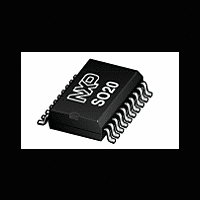
BUK9MRR-65PKK NXP Semiconductors, BUK9MRR-65PKK Datasheet - Page 9

BUK9MRR-65PKK
Manufacturer Part Number
BUK9MRR-65PKK
Description
Dual N-channel enhancement mode field-effect power transistor in SO20
Manufacturer
NXP Semiconductors
Datasheet
1.BUK9MRR-65PKK.pdf
(17 pages)
NXP Semiconductors
Table 6.
BUK9MRR-65PKK
Product data sheet
Symbol
L
FET1 and FET2 source-drain diode
V
t
Q
rr
Fig 9.
S
SD
r
R
(mΩ)
DSon
120
100
80
60
40
of gate-source voltage; typical values, FET1
and FET2
Drain-source on-state resistance as a function
0
Characteristics
Parameter
internal source
inductance
source-drain voltage
reverse recovery time
recovered charge
2
4
…continued
6
Conditions
pad
I
see
I
V
All information provided in this document is subject to legal disclaimers.
S
S
8
from source lead to source bonding
GS
V
001aal787
= 10 A; V
= 3 A; dI
GS
Figure 21
= -10 V; V
(V)
10
Rev. 02 — 17 June 2010
S
GS
/dt = -100 A/µs;
DS
= 0 V; T
= 30 V
Fig 10. Forward transconductance as a function of
j
= 25 °C;
(S )
g
fs
60
50
40
30
20
drain current; typical values, FET1 and FET2
0
Dual TrenchPLUS FET Logic Level FET
BUK9MRR-65PKK
5
Min
-
-
-
-
10
Typ
2
0.85
41.4
0.087
© NXP B.V. 2010. All rights reserved.
003a a d897
I
D
Max
-
1.2
-
-
(A)
15
Unit
nH
V
ns
nC
9 of 17


