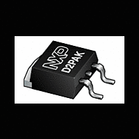
PSMN050-80BS NXP Semiconductors, PSMN050-80BS Datasheet - Page 6

PSMN050-80BS
Manufacturer Part Number
PSMN050-80BS
Description
Manufacturer
NXP Semiconductors
Datasheet
1.PSMN050-80BS.pdf
(14 pages)
NXP Semiconductors
Tested to JEDEC standards where applicable.
PSMN050-80BS
Product data sheet
Table 6.
Symbol
Source-drain diode
V
t
Q
rr
Fig 5.
Fig 7.
SD
r
1000
(pF)
(A)
C
800
600
400
200
I
40
30
20
10
D
0
0
function of drain-source voltage; typical values
function of gate-source voltage; typical values
Output characteristics: drain current as a
Input and reverse transfer capacitances as a
0
2
Characteristics
C
C
iss
rss
20
Parameter
source-drain voltage
reverse recovery time
recovered charge
2
10
4
8
6
4
…continued
6
6
V
GS
8
(V) =
Conditions
I
see
I
V
All information provided in this document is subject to legal disclaimers.
S
S
8
V
5.5
DS
003aad046
003aad052
V
GS
= 15 A; V
= 50 A; dI
DS
Figure 16
(V)
= 40 V
4.5
(V)
5
10
10
Rev. 1 — 2 March 2012
GS
S
/dt = 100 A/µs; V
= 0 V; T
N-channel 80 V 46 mΩ standard level MOSFET in D2PAK
Fig 6.
Fig 8.
j
= 25 °C;
(S)
g
R
(mΩ)
fs
DSon
100
35
30
25
20
15
10
80
60
40
20
5
0
GS
of drain current; typical values
drain current; typical values
Drain-source on-state resistance as a function
Forward transconductance as a function of
0
0
= 0 V;
V
10
GS
10
(V) =
PSMN050-80BS
20
5
Min
-
-
-
20
30
Typ
0.86
32
28
30
5.5
© NXP B.V. 2012. All rights reserved.
40
003aad047
003aad053
I
D
I
D
6
(A)
Max
1.2
-
-
(A)
20
8
10
40
50
nC
Unit
V
ns
6 of 14


