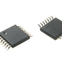
74VHCT541ATTR STMicroelectronics, 74VHCT541ATTR Datasheet

74VHCT541ATTR
Specifications of 74VHCT541ATTR
74VHCT541ATTR
74VHCT541ATTRTR
74VHCT541ATTRTR
Available stocks
Related parts for 74VHCT541ATTR
74VHCT541ATTR Summary of contents
Page 1
... TTL threshold. MOS technology. All inputs and outputs are equipped with protection circuits against static discharge, giving them 2KV ESD immunity and transient excess voltage. 74VHCT541A OCTAL BUS BUFFER SOP TSSOP PACKAGE T & R SOP 74VHCT541AMTR TSSOP 74VHCT541ATTR Rev. 4 1/12 ...
Page 2
Figure 2: Input Equivalent Circuit Table 3: Truth Table Don’t Care Z : High impedance Table 4: Absolute Maximum Ratings Symbol V Supply Voltage Input Voltage ...
Page 3
Table 5: Recommended Operating Conditions Symbol V Supply Voltage CC V Input Voltage I V Output Voltage (see note Output Voltage (see note Operating Temperature op Input Rise and Fall Time (see note 3) ...
Page 4
Table 8: Capacitive Characteristics Symbol Parameter C Input Capacitance IN Output C OUT Capacitance C Power Dissipation PD Capacitance (note defined as the value of the IC’s internal equivalent capacitance which is calculated from the ...
Page 5
Figure 3: Test Circuit PLH PHL PZL PLZ PZH PHZ C =15/50pF or equivalent (includes jig and probe capacitance equivalent ...
Page 6
Figure 5: Waveform - Output Enable And Disable Time (f=1MHz; 50% duty cycle) 6/12 ...
Page 7
SO-20 MECHANICAL DATA DIM. MIN. A 2.35 A1 0.1 B 0.33 C 0.23 D 12. 10.00 h 0.25 L 0.4 k 0° ddd mm. TYP MAX. 2.65 0.093 0.30 0.004 0.51 0.013 0.32 0.009 13.00 0.496 ...
Page 8
DIM. MIN 0.05 A2 0.8 b 0.19 c 0.09 D 6.4 E 6 0˚ PIN 1 IDENTIFICATION 1 8/12 TSSOP20 MECHANICAL DATA mm. TYP MAX. 1.2 0.15 ...
Page 9
Tape & Reel SO-20 MECHANICAL DATA DIM. MIN 12 10.8 Bo 13.2 Ko 3.1 Po 3.9 P 11.9 mm. TYP MAX. 330 13.2 0.504 0.795 2.362 30.4 11 0.425 13.4 0.520 3.3 ...
Page 10
Tape & Reel TSSOP20 MECHANICAL DATA DIM. MIN 12 6.8 Bo 6.9 Ko 1.7 Po 3.9 P 11.9 10/12 mm. TYP MAX. 330 13.2 0.504 0.795 2.362 22.4 7 0.268 7.1 ...
Page 11
Table 10: Revision History Date Revision 16-Dec-2004 4 Description of Changes Order Codes Revision - pag. 1. 74VHCT541A 11/12 ...
Page 12
... No license is granted by implication or otherwise under any patent or patent rights of STMicroelectronics. Specifications mentioned in this publication are subject to change without notice. This publication supersedes and replaces all information previously supplied. STMicroelectronics products are not authorized for use as critical components in life support devices or systems without express written approval of STMicroelectronics ...


