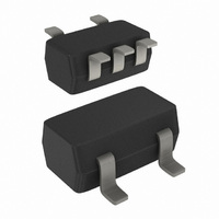
74HC1G126GW,125 NXP Semiconductors, 74HC1G126GW,125 Datasheet - Page 2

74HC1G126GW,125
Manufacturer Part Number
74HC1G126GW,125
Description
IC BUS BUFF DVR TRI-ST 5TSSOP
Manufacturer
NXP Semiconductors
Series
74HCr
Datasheet
1.74HCT1G126GV125.pdf
(12 pages)
Specifications of 74HC1G126GW,125
Package / Case
SC-70-5, SC-88A, SOT-323-5, SOT-353, 5-TSSOP
Logic Type
Buffer/Line Driver, Non-Inverting
Number Of Elements
1
Number Of Bits Per Element
1
Current - Output High, Low
7.8mA, 7.8mA
Voltage - Supply
2 V ~ 6 V
Operating Temperature
-40°C ~ 125°C
Mounting Type
Surface Mount
Logic Family
HC
Number Of Channels Per Chip
1
Polarity
Non-Inverting
Supply Voltage (max)
6 V
Supply Voltage (min)
2 V
Maximum Operating Temperature
+ 125 C
Mounting Style
SMD/SMT
High Level Output Current
- 7.8 mA
Low Level Output Current
7.8 mA
Minimum Operating Temperature
- 40 C
Output Type
3-State
Propagation Delay Time
24 ns (Typ) @ 2 V or 10 ns (Typ) @ 4.5 V or 9 ns (Typ) @ 6 V
Number Of Lines (input / Output)
1 / 1
Logical Function
Buffer/Line Driver
Number Of Elements
1
Number Of Channels
1
Number Of Inputs
1
Number Of Outputs
1
Operating Supply Voltage (typ)
5V
Package Type
TSSOP
Operating Supply Voltage (max)
6V
Operating Supply Voltage (min)
2V
Quiescent Current
20uA
Technology
CMOS
Pin Count
5
Mounting
Surface Mount
Operating Temp Range
-40C to 125C
Operating Temperature Classification
Automotive
Lead Free Status / RoHS Status
Lead free / RoHS Compliant
Lead Free Status / RoHS Status
Lead free / RoHS Compliant, Lead free / RoHS Compliant
Other names
74HC1G126GW-G
74HC1G126GW-G
935245710125
74HC1G126GW-G
935245710125
NXP Semiconductors
5. Functional diagram
6. Pinning information
Table 3.
7. Functional description
Table 4.
H = HIGH voltage level; L = LOW voltage level; X = don’t care; Z = high-impedance OFF-state
74HC_HCT1G126_4
Product data sheet
Symbol
OE
A
GND
Y
V
Inputs
OE
H
H
L
Fig 1. Logic symbol
Fig 4. Pin configuration
CC
2
1
Pin description
Function table
A
OE
6.1 Pinning
6.2 Pin description
mna125
Y
Pin
1
2
3
4
5
4
A
L
H
X
Fig 2. IEC logic symbol
GND
OE
A
Rev. 04 — 20 July 2007
2
1
Description
output enable input
data input
ground (0 V)
data output
supply voltage
1
2
3
74HCT1G126
OE
74HC1G126
001aaf103
74HC1G126; 74HCT1G126
mna126
5
4
4
V
Y
CC
Output
Y
L
H
Z
Fig 3. Logic diagram
OE
A
Bus buffer/line driver; 3-state
© NXP B.V. 2007. All rights reserved.
mna127
2 of 12
Y


