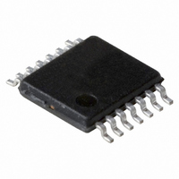
74LVC126APW/DG,118 NXP Semiconductors, 74LVC126APW/DG,118 Datasheet

74LVC126APW/DG,118
Specifications of 74LVC126APW/DG,118
74LVC126APW/DG-T
935283542118
Related parts for 74LVC126APW/DG,118
74LVC126APW/DG,118 Summary of contents
Page 1
Quad buffer/line driver with 5 V tolerant input/outputs; 3-state Rev. 06.00 — 16 May 2006 1. General description The 74LVC126A consists of four non-inverting buffers/line drivers with 3-state outputs, which are controlled by the output enable input (nOE). A ...
Page 2
Philips Semiconductors 4. Functional diagram 1OE 2OE 3OE 4OE 13 mna235 Fig 1. Logic symbol Fig 3. Logic diagram 5. Pinning information 5.1 Pinning 1OE ...
Page 3
Philips Semiconductors 5.2 Pin description Table 2: Pin description Symbol Pin Description 1OE 1 data enable input (active HIGH data input 1Y 3 data output 2OE 4 data enable input (active HIGH data input 2Y 6 ...
Page 4
Philips Semiconductors 7. Limiting values Table 4: Limiting values In accordance with the Absolute Maximum Rating System (IEC 60134). Symbol Parameter V supply voltage CC I input clamping current IK V input voltage I I output clamping current OK V ...
Page 5
Philips Semiconductors 9. Static characteristics Table 6: Static characteristics At recommended operating conditions. Voltages are referenced to GND (ground = 0 V). Symbol Parameter = −40 °C to +85 °C T amb V HIGH-level input voltage LOW-level ...
Page 6
Philips Semiconductors …continued Table 6: Static characteristics At recommended operating conditions. Voltages are referenced to GND (ground = 0 V). Symbol Parameter V HIGH-level output OH voltage V LOW-level output OL voltage I input leakage current I I OFF-state output ...
Page 7
Philips Semiconductors Table 7: Dynamic characteristics Voltages are referenced to GND (ground = 0 V). For test circuit see Symbol Parameter HIGH to OFF-state, LOW to PHZ PLZ OFF-state propagation delay nOE output skew ...
Page 8
Philips Semiconductors Σ(C × × sum of the outputs 11. AC waveforms ≥ 0.5 × < 2.7 ...
Page 9
Philips Semiconductors negative positive Test data is given in Table 9. Definitions for test circuit Load resistance Load capacitance including jig and probe capacitance Termination resistance should be equal to output impedance ...
Page 10
Philips Semiconductors 12. Package outline SO14: plastic small outline package; 14 leads; body width 3 pin 1 index 1 e DIMENSIONS (inch dimensions are derived from the original mm dimensions) A UNIT ...
Page 11
Philips Semiconductors SSOP14: plastic shrink small outline package; 14 leads; body width 5 pin 1 index 1 e DIMENSIONS (mm are the original dimensions) A UNIT max. 0.21 1.80 ...
Page 12
Philips Semiconductors TSSOP14: plastic thin shrink small outline package; 14 leads; body width 4 pin 1 index 1 e DIMENSIONS (mm are the original dimensions) A UNIT max. 0.15 0.95 ...
Page 13
Philips Semiconductors DHVQFN14: plastic dual in-line compatible thermal enhanced very thin quad flat package; no leads; 14 terminals; body 2 0.85 mm terminal 1 index area terminal 1 index area ...
Page 14
Philips Semiconductors 13. Abbreviations Table 10. Abbreviations Acronym Description CDM Charged Device Model CMOS Complementary Metal Oxide Semiconductor DUT Device Under Test ESD ElectroStatic Discharge HBM Human Body Model TTL Transistor Transistor Logic 14. Revision history Table 11. Revision history ...
Page 15
Philips Semiconductors 15. Legal information 15.1 Data sheet status [1][2] Document status Product status Objective [short] data sheet Development Preliminary [short] data sheet Qualification Product [short] data sheet Production [1] Please consult the most recently issued document before initiating or ...
Page 16
Philips Semiconductors 17. Contents 1 General description . . . . . . . . . . . . . . . . . . . . . . 1 2 Features . . . . . . . . ...


