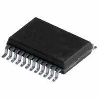
74LVC827ADB,112 NXP Semiconductors, 74LVC827ADB,112 Datasheet - Page 9

74LVC827ADB,112
Manufacturer Part Number
74LVC827ADB,112
Description
IC BUFF DVR TRI-ST 10BIT 24SSOP
Manufacturer
NXP Semiconductors
Series
74LVCr
Datasheet
1.74LVC827APW118.pdf
(17 pages)
Specifications of 74LVC827ADB,112
Logic Type
Buffer/Line Driver, Non-Inverting
Number Of Elements
1
Number Of Bits Per Element
10
Current - Output High, Low
24mA, 24mA
Voltage - Supply
2.7 V ~ 3.6 V
Operating Temperature
-40°C ~ 125°C
Mounting Type
Surface Mount
Package / Case
24-SSOP
Logic Family
LVC
Number Of Channels Per Chip
10
Polarity
Non-Inverting
Supply Voltage (max)
3.6 V
Supply Voltage (min)
1.2 V
Maximum Operating Temperature
+ 125 C
Mounting Style
SMD/SMT
High Level Output Current
- 24 mA
Low Level Output Current
24 mA
Minimum Operating Temperature
- 40 C
Number Of Lines (input / Output)
10 / 10
Output Type
3-State
Propagation Delay Time
10 ns at 1.2 V, 2.8 ns at 3.3 V
Lead Free Status / RoHS Status
Lead free / RoHS Compliant
Other names
74LVC827ADB
74LVC827ADB
935262419112
74LVC827ADB
935262419112
Philips Semiconductors
Table 8:
GND = 0 V; see
[1]
[2]
[3]
[4]
[5]
9397 750 13037
Product data sheet
Symbol
t
t
C
T
t
t
t
t
PHZ
sk(0)
PHL
PZH
PHZ
sk(0)
amb
PD
, t
, t
, t
, t
All typical values are measured T
These typical values are measured at V
Skew between any two outputs of the same package switching in the same direction. This parameter is guaranteed by design.
C
P
f
f
C
V
N = total load switching outputs;
The condition is V
i
o
(C
D
CC
= 40 C to +125 C
PD
= input frequency in MHz;
L
PLZ
PLH
PZL
PLZ
= output frequency in MHz;
= output load capacitance in pF;
= C
L
is used to determine the dynamic power dissipation (P
= supply voltage in V;
PD
V
Dynamic Characteristics
CC
Parameter
3-state output disable
time OEn to Yn
skew
power dissipation
capacitance per buffer
propagation delay
An to Yn
3-state output enable
time OEn to Yn
3-state output disable
time OEn to Yn
skew
2
V
CC
Figure
f
o
2
) = sum of the outputs.
I
= GND to V
f
i
7.
N + (C
L
CC
.
amb
V
CC
Conditions
see
V
see
see
see
= 25 C.
2
CC
…continued
V
V
V
outputs enabled
outputs disabled
V
V
V
V
V
V
V
V
V
CC
CC
CC
CC
CC
CC
CC
CC
CC
CC
CC
CC
CC
Figure 6
Figure 5
Figure 6
Figure 6
f
= 3.3 V
o
= 3.3 V.
) where:
= 1.2 V
= 2.7 V
= 3.0 V to 3.6 V
= 1.2 V
= 2.7 V
= 3.0 V to 3.6 V
= 1.2 V
= 2.7 V
= 3.0 V to 3.6 V
= 1.2 V
= 2.7 V
= 3.0 V to 3.6 V
10-bit buffer/line driver with 5 V tolerant inputs/outputs; 3-state
Rev. 02 — 8 April 2004
D
in W).
[4] [5]
[2]
[3]
[3]
Min
-
1.5
1.5
-
-
-
-
1.5
1.0
-
1.5
1.0
-
1.5
1.5
-
© Koninklijke Philips Electronics N.V. 2004. All rights reserved.
Typ
10.0
-
2.9
-
12
3
-
-
-
-
-
-
-
-
-
-
74LVC827A
Max
-
7.3
6.7
1.0
-
-
-
9.0
8.5
-
11.0
9.5
-
9.5
8.5
1.5
Unit
ns
ns
ns
ns
pF
pF
ns
ns
ns
ns
ns
ns
ns
ns
ns
ns
9 of 17


