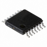
74AHCT125PW,112 NXP Semiconductors, 74AHCT125PW,112 Datasheet - Page 2

74AHCT125PW,112
Manufacturer Part Number
74AHCT125PW,112
Description
IC BUFF/DVR 3-ST QUAD 14-TSSOP
Manufacturer
NXP Semiconductors
Series
74AHCTr
Datasheet
1.74AHC125PW118.pdf
(15 pages)
Specifications of 74AHCT125PW,112
Logic Type
Buffer/Line Driver, Non-Inverting
Number Of Elements
4
Number Of Bits Per Element
1
Current - Output High, Low
8mA, 8mA
Voltage - Supply
4.5 V ~ 5.5 V
Operating Temperature
-40°C ~ 125°C
Mounting Type
Surface Mount
Package / Case
14-TSSOP
Logic Family
AHCT
Number Of Channels Per Chip
4
Polarity
Non-Inverting
Supply Voltage (max)
5.5 V
Supply Voltage (min)
4.5 V
Maximum Operating Temperature
+ 125 C
Mounting Style
SMD/SMT
High Level Output Current
- 8 mA
Low Level Output Current
8 mA
Minimum Operating Temperature
- 40 C
Number Of Lines (input / Output)
4 / 4
Output Type
3-State
Propagation Delay Time
7.5 ns at 4.5 V to 5.5 V
Lead Free Status / RoHS Status
Lead free / RoHS Compliant
Other names
568-4844-5
74AHCT125PW
74AHCT125PW,112
74AHCT125PW
935262765112
74AHCT125PW
74AHCT125PW,112
74AHCT125PW
935262765112
NXP Semiconductors
4. Functional diagram
5. Pinning information
74AHC_AHCT125_4
Product data sheet
Fig 1. Logic symbol
Fig 4. Pin configuration SO14 and TSSOP14
10
12
13
2
1
5
4
9
GND
1OE
2OE
1A
1Y
2A
2Y
1OE
2OE
3OE
4OE
1A
2A
3A
4A
5.1 Pinning
1
2
3
4
5
6
7
mna228
1Y
2Y
3Y
4Y
74AHCT125
74AHC125
11
3
6
8
001aae755
14
13
12
11
10
9
8
Fig 2. IEC logic symbol
V
4OE
4A
4Y
3OE
3A
3Y
CC
Rev. 04 — 11 January 2008
10
13
12
2
1
5
4
9
EN1
mna229
1
Fig 5. Pin configuration DHVQFN14
(1) The die substrate is attached to this pad using
74AHC125; 74AHCT125
11
3
6
8
conductive die attach material. It can not be used as
a supply pin or input.
index area
terminal 1
2OE
1A
1Y
2A
2Y
Fig 3. Logic diagram (one buffer)
nOE
Transparent top view
2
3
4
5
6
nA
Quad buffer/line driver; 3-state
74AHCT125
74AHC125
GND
(1)
13
12
11
10
9
001aah082
© NXP B.V. 2008. All rights reserved.
4OE
4A
4Y
3OE
3A
mna227
2 of 15
nY


