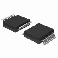
74HCT40105DB,118 NXP Semiconductors, 74HCT40105DB,118 Datasheet - Page 2

74HCT40105DB,118
Manufacturer Part Number
74HCT40105DB,118
Description
IC FIFO REGISTER 4X16 16SSOP
Manufacturer
NXP Semiconductors
Series
74HCTr
Datasheet
1.74HC40105DB118.pdf
(25 pages)
Specifications of 74HCT40105DB,118
Function
Asynchronous
Memory Size
64 (4 x 16)
Data Rate
25MHz
Voltage - Supply
4.5 V ~ 5.5 V
Mounting Type
Surface Mount
Package / Case
16-SSOP
Lead Free Status / RoHS Status
Lead free / RoHS Compliant
Operating Temperature
-
Access Time
-
Other names
74HCT40105DB-T
74HCT40105DB-T
935189960118
74HCT40105DB-T
935189960118
Philips Semiconductors
FEATURES
GENERAL DESCRIPTION
The 74HC/HCT40105 are high-speed Si-gate CMOS
devices and are pin compatible with the “40105” of the
“4000B” series. They are specified in compliance with
JEDEC standard no. 7A.
The 74HC/HCT40105 are first-in/first-out (FIFO) “elastic”
storage registers that can store sixteen 4-bit words. The
“40105” is capable of handling input and output data at
QUICK REFERENCE DATA
GND = 0 V; T
Notes
1. C
2. For HC the condition is V
1998 Jan 23
t
t
f
C
C
PHL
PHL
max
SYMBOL
Independent asynchronous inputs and outputs
Expandable in either direction
Reset capability
Status indicators on inputs and outputs
3-state outputs
Output capability: standard
I
I
PD
4-bit x 16-word FIFO register
CC
For HCT the condition is V
/ t
PD
category: MSI
PLH
P
f
f
C
V
i
o
is used to determine the dynamic power dissipation (P
D
CC
= input frequency in MHz.
L
= output frequency in MHz.
(C
= output load capacitance in pF
= C
L
= supply voltage in V
amb
PD
propagation delay
propagation delay
maximum clock frequency
input capacitance
power dissipation capacitance per package
V
MR to DIR, DOR
SO to Q
SI to DIR
SO to DOR
CC
= 25 C; t
V
2
CC
f
2
o
) = sum of outputs
n
f
r
i
= t
PARAMETER
I
I
f
= GND to V
= GND to V
= 6 ns
(C
L
V
CC
2
CC
CC
f
o
) where:
1.5
2
C
notes 1 and 2
different shifting rates. This feature makes it particularly
useful as a buffer between asynchronous systems. Each
word position in the register is clocked by a control flip-flop,
which stores a marker bit. A “1” signifies that the position’s
data is filled and a “0” denotes a vacancy in that position.
The control flip-flop detects the state of the preceding
flip-flop and communicates its own status to the
succeeding flip-flop. When a control flip-flop is in the “0”
state and sees a “1” in the preceding flip-flop, it generates
a clock pulse that transfers data from the preceding four
data latches into its own four data latches and resets the
preceding flip-flop to “0”. The first and last control flip-flops
have buffered outputs. Since all empty locations “bubble”
automatically to the input end, and all valid data ripples
through to the output end, the status of the first control
flip-flop (data-in ready output - DIR) indicates if the FIFO is
full, and the status of the last flip-flop (data-out ready
output - DOR) indicates if the FIFO contains data. As the
earliest data is removed from the bottom of the data stack
(output end), all data entered later will automatically ripple
toward the output.
L
D
= 15 pF; V
in W):
CONDITIONS
CC
= 5 V
16
37
16
17
33
3.5
134
74HC/HCT40105
HC
Product specification
TYP.
15
35
18
18
31
3.5
145
HCT
ns
ns
ns
ns
MHz
pF
pF
UNIT


