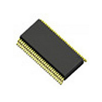
IDT72V82L20PA IDT, Integrated Device Technology Inc, IDT72V82L20PA Datasheet - Page 2

IDT72V82L20PA
Manufacturer Part Number
IDT72V82L20PA
Description
IC FIFO ASYNCH 1KX9 56TSSOP
Manufacturer
IDT, Integrated Device Technology Inc
Series
72Vr
Datasheet
1.IDT72V82L15PAG.pdf
(12 pages)
Specifications of IDT72V82L20PA
Function
Asynchronous
Memory Size
9K (1K x 9)
Data Rate
33MHz
Access Time
20ns
Voltage - Supply
3 V ~ 3.6 V
Operating Temperature
0°C ~ 70°C
Mounting Type
Surface Mount
Package / Case
56-TSSOP
Configuration
Dual
Density
18Kb
Access Time (max)
20ns
Word Size
9b
Organization
1Kx9x2
Sync/async
Asynchronous
Expandable
Yes
Bus Direction
Bi-Directional
Package Type
TSSOP
Clock Freq (max)
Not RequiredMHz
Operating Supply Voltage (typ)
3.3V
Operating Supply Voltage (min)
3V
Operating Supply Voltage (max)
3.6V
Supply Current
100mA
Operating Temp Range
0C to 70C
Operating Temperature Classification
Commercial
Mounting
Surface Mount
Pin Count
56
Lead Free Status / RoHS Status
Contains lead / RoHS non-compliant
Other names
72V82L20PA
Available stocks
Company
Part Number
Manufacturer
Quantity
Price
Part Number:
IDT72V82L20PA
Manufacturer:
IDT
Quantity:
20 000
PIN CONFIGURATION
DC ELECTRICAL
CHARACTERISTICS
(Commercial: V
NOTES:
1. Measurements with 0.4 ≤ V
2. R ≥ V
3. Tested with outputs open (I
4. Tested at f = 20 MHz.
5. All Inputs = V
Symbol
IDT72V81/72V82/72V83/72V84/72V85 3.3V CMOS DUAL ASYNCHRONOUS FIFO
512 x 9, 1024 x 9, 2048 x 9, 4096 x 9, 8192 x 9
I
I
V
V
I
I
CC1
CC2
LI
LO
XOA/HFA
XOB/HFB
OH
OL
(1)
(2)
(3,4)
(3,5)
GND
GND
IH
FFA
EFA
FFB
EFB
QA
QA
QA
QA
QA
QA
QA
QA
QA
QB
QB
QB
QB
QB
QB
QB
QB
QB
, 0.4 ≤ V
RA
RB
Input Leakage Current (Any Input)
Output Leakage Current
Output Logic “1” Voltage
I
Output Logic “0” Voltage
I
Active Power Supply Current (both FIFOs)
Standby Current (R=W=RS=FL/RT=V
OH
OL
0
1
2
3
8
4
5
6
7
0
1
2
3
8
4
5
6
7
CC
= –2mA
= 8mA
CC
- 0.2V or GND + 0.2V.
OUT
= 3.3V±0.3V, T
1
2
3
4
5
6
7
8
9
10
11
12
13
14
15
16
17
18
19
20
21
22
23
24
25
26
27
28
≤ V
TSSOP (SO56-2, order code: PA)
CC
Parameter
OUT
.
IN
= 0).
≤ V
TOP VIEW
A
CC
= 0°C to +70°C)
.
(1)
IH
)
56
55
54
53
52
51
50
49
48
47
46
45
44
43
42
41
40
39
38
37
36
35
34
33
32
31
30
29
–10
2.4
t
Min.
–1
—
—
—
Commercial
A
IDT72V81
IDT72V82
IDT72V83
IDT72V84
IDT72V85
= 15, 20 ns
XIA
DA
DA
DA
DA
DA
WA
V
DA
DA
DA
DA
FLA/RTA
RSA
XIB
DB
DB
DB
DB
DB
WB
V
DB
DB
DB
DB
FLB/RTB
RSB
3966 drw 02
CC
CC
0
1
2
3
8
4
5
6
7
0
1
2
3
8
4
5
6
7
Max.
100
0.4
10
—
1
5
Unit
µA
µA
mA
mA
V
V
2
CAPACITANCE
NOTE:
1. Characterized values, not currently tested.
ABSOLUTE MAXIMUM RATINGS
NOTE:
1. Stresses greater than those listed under ABSOLUTE MAXIMUM RATINGS may cause
RECOMMENDED DC OPERATING
CONDITIONS
NOTES:
1. For RT/RS/XI input, V
2. 1.5V undershoots are allowed for 10ns once per cycle.
AC TEST CONDITIONS
Symbol
Symbol
C
C
V
GND
V
V
T
Symbol
V
T
I
A
IN
OUT
CC
Input Pulse Levels
Input Rise/Fall Times
Input Timing Reference Levels
Output Reference Levels
Output Load
OUT
permanent damage to the device. This is a stress rating only and functional operation of
the device at these or any other conditions above those indicated in the operational
sections of this specification is not implied. Exposure to absolute maximum rating
conditions for extended periods may affect reliability.
IH
IL
STG
TERM
(2)
(1)
Supply Voltage
Supply Voltage
Input High Voltage
Input Low Voltage
Operating Temperature
Commercial
Terminal Voltage
with Respect to GND
Storage Temperature
DC Output Current
Output Capacitance
Input Capacitance
*Includes scope and jib capacitances.
OUTPUT
Parameter
Parameter
IH
Rating
= 2.6V (commercial).
PIN
Figure 1. Output Load
TO
510Ω
or equivalent circuit
(T
(1)
COMMERCIAL TEMPERATURE RANGE
A
= +25°C, f = 1.0 MHz)
V
Condition
3.3V
Min.
V
OUT
3.0
2.0
—
IN
0
0
= 0V
330Ω
30pF*
Commercial
–0.5 to +7.0
–55 to +125
= 0V
–50 to +50
Typ.
3.3
—
—
—
0
3966 drw 03
FEBRUARY 5, 2009
GND to 3.0V
See Figure 1
1.5V
1.5V
5ns
Max.
V
CC
Max.
8
8
3.6
0.8
70
0
+0.5
Unit
Unit
mA
°C
pF
pF
V
Unit
°C
V
V
V
V


