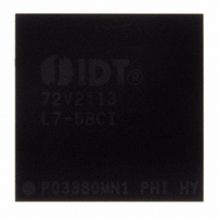
IDT72V2113L7-5BCI IDT, Integrated Device Technology Inc, IDT72V2113L7-5BCI Datasheet - Page 26

IDT72V2113L7-5BCI
Manufacturer Part Number
IDT72V2113L7-5BCI
Description
IC FIFO SYNC 3.3V 5NS 100-LBGA
Manufacturer
IDT, Integrated Device Technology Inc
Series
72Vr
Datasheet
1.IDT72V2103L15PF8.pdf
(46 pages)
Specifications of IDT72V2113L7-5BCI
Function
Synchronous
Memory Size
4.7Mb (262k x 18)
Access Time
5ns
Voltage - Supply
3.15 V ~ 3.45 V
Operating Temperature
-40°C ~ 85°C
Mounting Type
Surface Mount
Package / Case
100-LBGA
Configuration
Dual
Density
4.5Mb
Access Time (max)
5ns
Word Size
18/9Bit
Organization
256Kx18/512Kx9
Sync/async
Synchronous
Expandable
Yes
Bus Direction
Uni-Directional
Clock Freq (max)
133.3MHz
Operating Supply Voltage (typ)
3.3V
Operating Supply Voltage (min)
3.15V
Operating Supply Voltage (max)
3.45V
Supply Current
35mA
Operating Temp Range
-40C to 85C
Operating Temperature Classification
Industrial
Mounting
Surface Mount
Pin Count
100
Lead Free Status / RoHS Status
Contains lead / RoHS non-compliant
Data Rate
-
Lead Free Status / RoHS Status
Not Compliant, Contains lead / RoHS non-compliant
Other names
72V2113L7-5BCI
800-1513
800-1513
Available stocks
Company
Part Number
Manufacturer
Quantity
Price
Company:
Part Number:
IDT72V2113L7-5BCI
Manufacturer:
IDT, Integrated Device Technology Inc
Quantity:
10 000
Q
D
NOTES:
1. t
2. LD = HIGH.
3. First data word latency: t
NOTES:
1. t
2. LD = HIGH, EF = HIGH
IDT72V2103/72V2113 3.3V HIGH DENSITY SUPERSYNC II
IDT72V263/273/283/293/103/113 3.3V HIGH DENSITY SUPERSYNC II
8K x 18, 16K x 9/18, 32K x 9/18, 64K x 9/18, 128K x 9/18, 256K x 9/18, 512K x9
131,072 x 18/262,144 x 9, 262,144 x 18/524,288 x 9
D
Q
WCLK
RCLK
0
0
WEN
WCLK
REN
0
0
RCLK
- Q
- D
of WCLK and the rising edge of RCLK is less than t
of the RCLK and the rising edge of the WCLK is less than t
SKEW1
WEN
SKEW1
OE
REN
EF
- D
- Q
FF
n
n
n
n
is the minimum time between a rising WCLK edge and a rising RCLK edge to guarantee that EF will go HIGH (after one RCLK cycle plus t
t
is the minimum time between a rising RCLK edge and a rising WCLK edge to guarantee that FF will go high (after one WCLK cycle pus t
ENS
DATA IN OUTPUT REGISTER
t
ENS
t
SKEW1
t
t
OLZ
ENH
SKEW1
t
REF
t
A
Figure 8. Read Cycle, Empty Flag and First Data Word Latency Timing (IDT Standard Mode)
t
OE
(1)
+ 1*T
t
SKEW1
RCLK
t
t
ENS
ENH
t
DS
t
A
+ t
D
(1)
1
0
REF
NO WRITE
NO OPERATION
Figure 7. Write Cycle and Full Flag Timing (IDT Standard Mode)
.
t
t
DHS
ENH
SKEW1
LAST WORD
1
, then EF deassertion may be delayed one extra RCLK cycle.
SKEW1
2
t
, then the FF deassertion may be delayed one extra WCLK cycle.
WFF
TM
t
t
OHZ
DS
t
NARROW BUS FIFO
t
DS
ENS
D
DX
1
NO OPERATION
TM
t
CLKH
t
WFF
NARROW BUS FIFO
t
t
ENH
DH
DATA READ
26
t
t
DH
CLK
2
t
CLKL
t
CLKH
t
t
REF
ENS
t
OLZ
t
SKEW1
t
CLK
(1)
t
CLKL
t
ENS
t
ENH
LAST WORD
t
A
1
NO WRITE
t
ENH
t
A
COMMERCIAL AND INDUSTRIAL
WFF
REF
2
t
WFF
). If the time between the rising edge
). If the time between the rising edge
TEMPERATURE RANGES
t
ENS
t
DS
NEXT DATA READ
D
0
DX+1
JUNE 1, 2010
t
WFF
t
REF
t
t
ENH
A
6119 drw10
t
DH
6119 drw11
D
1


