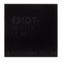
IDT72V2113L7-5BCI IDT, Integrated Device Technology Inc, IDT72V2113L7-5BCI Datasheet - Page 34

IDT72V2113L7-5BCI
Manufacturer Part Number
IDT72V2113L7-5BCI
Description
IC FIFO SYNC 3.3V 5NS 100-LBGA
Manufacturer
IDT, Integrated Device Technology Inc
Series
72Vr
Datasheet
1.IDT72V2103L15PF8.pdf
(46 pages)
Specifications of IDT72V2113L7-5BCI
Function
Synchronous
Memory Size
4.7Mb (262k x 18)
Access Time
5ns
Voltage - Supply
3.15 V ~ 3.45 V
Operating Temperature
-40°C ~ 85°C
Mounting Type
Surface Mount
Package / Case
100-LBGA
Configuration
Dual
Density
4.5Mb
Access Time (max)
5ns
Word Size
18/9Bit
Organization
256Kx18/512Kx9
Sync/async
Synchronous
Expandable
Yes
Bus Direction
Uni-Directional
Clock Freq (max)
133.3MHz
Operating Supply Voltage (typ)
3.3V
Operating Supply Voltage (min)
3.15V
Operating Supply Voltage (max)
3.45V
Supply Current
35mA
Operating Temp Range
-40C to 85C
Operating Temperature Classification
Industrial
Mounting
Surface Mount
Pin Count
100
Lead Free Status / RoHS Status
Contains lead / RoHS non-compliant
Data Rate
-
Lead Free Status / RoHS Status
Not Compliant, Contains lead / RoHS non-compliant
Other names
72V2113L7-5BCI
800-1513
800-1513
Available stocks
Company
Part Number
Manufacturer
Quantity
Price
Company:
Part Number:
IDT72V2113L7-5BCI
Manufacturer:
IDT, Integrated Device Technology Inc
Quantity:
10 000
NOTES:
1. n = PAE offset.
2. For IDT Standard mode
3. For FWFT mode.
4. t
5. PAE is asserted and updated on the rising edge of WCLK only.
6. Select this mode by setting PFM HIGH during Master Reset.
NOTES:
1. m = PAF offset.
2. D = maximum FIFO Depth.
are selected, D = 262,144 for the IDT72V2103 and 524,288 for the IDT72V2113.
selected, D = 262,145 for the IDT72V2103 and 524,289 for the IDT72V2113.
3. PAF is asserted to LOW on WCLK transition and reset to HIGH on RCLK transition.
4. Select this mode by setting PFM LOW during Master Reset.
WCLK
IDT72V2103/72V2113 3.3V HIGH DENSITY SUPERSYNC II
IDT72V263/273/283/293/103/113 3.3V HIGH DENSITY SUPERSYNC II
8K x 18, 16K x 9/18, 32K x 9/18, 64K x 9/18, 128K x 9/18, 256K x 9/18, 512K x9
131,072 x 18/262,144 x 9, 262,144 x 18/524,288 x 9
RCLK
WCLK
RCLK
WEN
edge of WCLK and the rising edge of RCLK is less than t
In IDT Standard mode: if x18 Input or x18 Output bus Width is selected, D = 131,072 for the IDT72V2103 and 262,144 for the IDT72V2113. If both x9 Input and x9 Output bus Widths
In FWFT mode: if x18 Input or x18 Output bus Width is selected, D = 131,073 for the IDT72V2103 and 262,145 for the DT72V2113. If both x9 Input and x9 Output bus Widths are
WEN
REN
REN
SKEW2
PAF
PAE
is the minimum time between a rising WCLK edge and a rising RCLK edge to guarantee that PAE will go HIGH (after one RCLK cycle plus t
t
CLKH
Figure 19. Synchronous Programmable Almost-Empty Flag Timing (IDT Standard and FWFT Modes)
Figure 20. Asynchronous Programmable Almost-Full Flag Timing (IDT Standard and FWFT Modes)
t
ENS
n words in FIFO
n+1 words in FIFO
t
CLKL
D ⎯ (m + 1) words in FIFO
t
ENH
t
SKEW2
(2)
1
,
(3)
(4)
t
PAES
SKEW2
t
CLKH
, then the PAE deassertion may be delayed one extra RCLK cycle.
2
TM
NARROW BUS FIFO
t
ENS
t
CLKL
TM
NARROW BUS FIFO
34
t
ENS
t
t
PAFA
ENH
n+1 words in FIFO
n+2 words in FIFO
t
ENS
t
ENH
D ⎯ m words
in FIFO
(2)
(3)
,
t
PAFA
1
COMMERCIAL AND INDUSTRIAL
t
PAES
PAES
TEMPERATURE RANGES
). If the time between the rising
2
words in FIFO
D ⎯ (m + 1)
n words in FIFO
n+1 words in FIFO
JUNE 1, 2010
6119 drw22
6119 drw23
(2)
,
(3)


