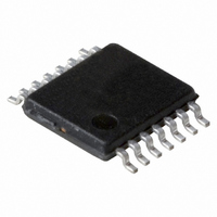
74LV74PW,118 NXP Semiconductors, 74LV74PW,118 Datasheet - Page 6

74LV74PW,118
Manufacturer Part Number
74LV74PW,118
Description
IC DUAL D FF POSEDG TRIG 14TSSOP
Manufacturer
NXP Semiconductors
Series
74LVr
Type
D-Typer
Specifications of 74LV74PW,118
Output Type
Differential
Package / Case
14-TSSOP
Function
Set(Preset) and Reset
Number Of Elements
2
Number Of Bits Per Element
1
Frequency - Clock
56MHz
Trigger Type
Positive Edge
Current - Output High, Low
12mA, 12mA
Voltage - Supply
1 V ~ 5.5 V
Operating Temperature
-40°C ~ 125°C
Mounting Type
Surface Mount
Number Of Circuits
2
Logic Family
LV
Logic Type
D-Type Edge Triggered Flip-Flop
Polarity
Inverting/Non-Inverting
Input Type
Single-Ended
Propagation Delay Time
11 ns at 3.3 V
High Level Output Current
- 12 mA
Low Level Output Current
12 mA
Supply Voltage (max)
5.5 V
Maximum Operating Temperature
+ 125 C
Mounting Style
SMD/SMT
Minimum Operating Temperature
- 40 C
Supply Voltage (min)
1 V
Delay Time - Propagation
-
Technology
CMOS
Number Of Bits
2
Number Of Elements
2
Clock-edge Trigger Type
Positive-Edge
Operating Supply Voltage (typ)
3.3V
Package Type
TSSOP
Frequency (max)
56MHz
Operating Supply Voltage (min)
1V
Operating Supply Voltage (max)
5.5V
Operating Temp Range
-40C to 125C
Operating Temperature Classification
Automotive
Mounting
Surface Mount
Pin Count
14
Lead Free Status / RoHS Status
Lead free / RoHS Compliant
Delay Time - Propagation
-
Lead Free Status / Rohs Status
Lead free / RoHS Compliant
Other names
74LV74PW-T
74LV74PW-T
935175140118
74LV74PW-T
935175140118
NXP Semiconductors
9. Static characteristics
Table 7.
Voltages are referenced to GND (ground = 0 V).
[1]
74LV74_3
Product data sheet
Symbol Parameter
V
V
V
V
I
I
C
I
CC
IH
IL
OH
OL
I
I
CC
Typical values are measured at T
HIGH-level input voltage
LOW-level input voltage
HIGH-level output voltage
LOW-level output voltage
input leakage current
supply current
additional supply current
input capacitance
Static characteristics
amb
= 25 C.
Conditions
V
V
V
V
V
V
V
V
V
V
V
V
V
V
per input; V
V
CC
CC
CC
CC
CC
CC
CC
CC
I
I
I
CC
I
CC
CC
l
l
l
l
l
l
l
I
I
I
I
I
I
I
= V
= V
= V
= V
O
O
O
O
O
O
O
O
O
O
O
O
O
O
= 1.2 V
= 2.0 V
= 1.2 V
= 2.0 V
= 2.7 V to 3.6 V
= 4.5 V to 5.5 V
= 2.7 V to 3.6 V
= 4.5 V to 5.5 V
= 5.5 V
= 5.5 V
= 2.7 V to 3.6 V
= 100 A; V
= 100 A; V
= 100 A; V
= 100 A; V
= 100 A; V
= 6 mA; V
= 12 mA; V
= 100 A; V
= 100 A; V
= 100 A; V
= 100 A; V
= 100 A; V
= 6 mA; V
= 12 mA; V
IH
IH
CC
CC
or V
or V
Rev. 03 — 28 September 2007
or GND;
or GND; I
I
IL
IL
= V
Dual D-type flip-flop with set and reset; positive edge-trigger
CC
CC
CC
CC
CC
CC
CC
CC
CC
CC
CC
CC
CC
CC
CC
= 3.0 V
O
= 3.0 V
= 4.5 V
= 1.2 V
= 2.0 V
= 2.7 V
= 3.0 V
= 4.5 V
= 4.5 V
= 0 A;
= 1.2 V
= 2.0 V
= 2.7 V
= 3.0 V
= 4.5 V
0.6 V;
0.7V
Min
0.9
1.4
2.0
1.8
2.5
2.8
4.3
2.4
3.6
-
-
-
-
-
-
-
-
-
-
-
-
-
-
-
-
CC
40 C to +85 C
Typ
2.82
0.25
0.35
1.2
2.0
2.7
3.0
4.5
4.2
3.5
0
0
0
0
0
-
-
-
-
-
-
-
-
-
-
-
[1]
0.3V
Max
0.40
0.55
500
0.3
0.6
0.8
0.2
0.2
0.2
0.2
1.0
20
-
-
-
-
-
-
-
-
-
-
-
-
-
CC
0.7V
40 C to +125 C Unit
Min
0.9
1.4
2.0
1.8
2.5
2.8
4.3
2.2
3.5
-
-
-
-
-
-
-
-
-
-
-
-
-
-
-
-
CC
© NXP B.V. 2007. All rights reserved.
74LV74
0.3V
Max
0.50
0.65
850
0.3
0.6
0.8
0.2
0.2
0.2
0.2
1.0
80
-
-
-
-
-
-
-
-
-
-
-
-
-
CC
V
V
V
V
V
V
V
V
V
V
V
V
V
V
V
V
V
V
V
V
V
V
pF
6 of 19
A
A
A


