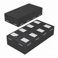
74LVC3G14GT,115 NXP Semiconductors, 74LVC3G14GT,115 Datasheet - Page 10

74LVC3G14GT,115
Manufacturer Part Number
74LVC3G14GT,115
Description
IC TRPL INV SCHMITT TRIG 8-XSON
Manufacturer
NXP Semiconductors
Series
74LVCr
Datasheet
1.74LVC3G17GD125.pdf
(23 pages)
Specifications of 74LVC3G14GT,115
Number Of Circuits
3
Logic Type
Inverter with Schmitt Trigger
Package / Case
8-XSON
Number Of Inputs
1
Current - Output High, Low
32mA, 32mA
Voltage - Supply
1.65 V ~ 5.5 V
Operating Temperature
-40°C ~ 125°C
Mounting Type
Surface Mount
Logic Family
LVC
High Level Output Current
- 32 mA
Low Level Output Current
32 mA
Propagation Delay Time
3.8 ns, 3.2 ns , 2.4 ns
Supply Voltage (max)
5.5 V
Supply Voltage (min)
1.65 V
Maximum Operating Temperature
+ 125 C
Mounting Style
SMD/SMT
Operating Supply Voltage
1.8 V, 2.5 V, 3.3 V, 5 V
Lead Free Status / RoHS Status
Lead free / RoHS Compliant
Lead Free Status / RoHS Status
Lead free / RoHS Compliant, Lead free / RoHS Compliant
Other names
74LVC3G14GT-G
74LVC3G14GT-G
935278934115
74LVC3G14GT-G
935278934115
NXP Semiconductors
15. Application information
74LVC3G14
Product data sheet
Fig 12. Typical transfer characteristics
V
CC
= 3.0 V
The slow input rise and fall times cause additional power dissipation, this can be
calculated using the following formula:
P
ΔI
An example of a relaxation circuit using the 74LVC3G14 is shown in
add
P
f
t
t
ΔI
CC(AV)
i
r
f
add
= input frequency (MHz);
= input fall time (ns); 90 % to 10 %;
= input rise time (ns); 10 % to 90 %;
CC(AV)
= f
= additional power dissipation (μW);
i
differs with positive or negative input transitions, as shown in
× (t
(mA)
I
CC
= average additional supply current (μA).
r
14
12
10
× ΔI
8
6
4
2
0
0
All information provided in this document is subject to legal disclaimers.
CC(AV)
Rev. 8 — 19 August 2010
+ t
0.5
f
× ΔI
CC(AV)
Triple inverting Schmitt trigger with 5 V tolerant input
1
) × V
CC
1.5
where:
V
mdb627
I
(V)
2
74LVC3G14
Figure
Figure
© NXP B.V. 2010. All rights reserved.
14.
13.
10 of 23


