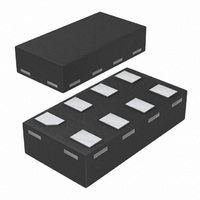
74LVC3G14GT,115 NXP Semiconductors, 74LVC3G14GT,115 Datasheet - Page 7

74LVC3G14GT,115
Manufacturer Part Number
74LVC3G14GT,115
Description
IC TRPL INV SCHMITT TRIG 8-XSON
Manufacturer
NXP Semiconductors
Series
74LVCr
Datasheet
1.74LVC3G17GD125.pdf
(23 pages)
Specifications of 74LVC3G14GT,115
Number Of Circuits
3
Logic Type
Inverter with Schmitt Trigger
Package / Case
8-XSON
Number Of Inputs
1
Current - Output High, Low
32mA, 32mA
Voltage - Supply
1.65 V ~ 5.5 V
Operating Temperature
-40°C ~ 125°C
Mounting Type
Surface Mount
Logic Family
LVC
High Level Output Current
- 32 mA
Low Level Output Current
32 mA
Propagation Delay Time
3.8 ns, 3.2 ns , 2.4 ns
Supply Voltage (max)
5.5 V
Supply Voltage (min)
1.65 V
Maximum Operating Temperature
+ 125 C
Mounting Style
SMD/SMT
Operating Supply Voltage
1.8 V, 2.5 V, 3.3 V, 5 V
Lead Free Status / RoHS Status
Lead free / RoHS Compliant
Lead Free Status / RoHS Status
Lead free / RoHS Compliant, Lead free / RoHS Compliant
Other names
74LVC3G14GT-G
74LVC3G14GT-G
935278934115
74LVC3G14GT-G
935278934115
NXP Semiconductors
Table 7.
At recommended operating conditions; voltages are referenced to GND (ground = 0 V).
[1]
Table 8.
Voltages are referenced to GND (ground = 0 V; for test circuit see
[1]
[2]
74LVC3G14
Product data sheet
Symbol Parameter
I
I
ΔI
Symbol Parameter
V
V
V
OFF
CC
T+
T−
H
CC
[2]
All typical values are measured at maximum V
All typical values are measured at T
V
H
= V
positive-going
threshold voltage
negative-going
threshold voltage
hysteresis voltage see
T+
power-off leakage current
supply current
additional supply current
Static characteristics
Transfer characteristics
− V
T−
Conditions
see
Figure 11
see
Figure 11
and
V
V
V
V
V
V
V
V
V
V
V
V
V
V
V
CC
CC
CC
CC
CC
CC
CC
CC
CC
CC
CC
CC
CC
CC
CC
Figure 10
Figure 10
Figure
Figure 12
…continued
amb
= 1.8 V
= 2.3 V
= 3.0 V
= 4.5 V
= 5.5 V
= 1.8 V
= 2.3 V
= 3.0 V
= 4.5 V
= 5.5 V
= 1.8 V
= 2.3 V
= 3.0 V
= 4.5 V
= 5.5 V
= 25 °C
Conditions
V
V
V
V
V
I
I
CC
I
CC
10,
All information provided in this document is subject to legal disclaimers.
or V
= 5.5 V or GND; I
= V
= 1.65 V to 5.5 V
= 2.3 V to 5.5 V
and
and
CC
Figure 11
CC
O
and T
= 5.5 V; V
− 0.6 V; I
Rev. 8 — 19 August 2010
amb
= 25 °C.
O
CC
O
= 0 A;
Triple inverting Schmitt trigger with 5 V tolerant input
= 0 V
= 0 A;
0.70
1.00
1.30
1.90
2.20
0.25
0.40
0.60
1.00
1.20
0.15
0.25
0.40
0.60
0.70
Figure 9
Min
−40 °C to +85 °C
Typ
1.10
1.40
1.76
2.47
2.91
0.61
0.80
1.04
1.55
1.86
0.49
0.60
0.73
0.92
1.02
[1]
Min
-
-
-
Max
1.50
1.80
2.20
3.10
3.60
0.90
1.15
1.50
2.00
2.30
1.00
1.10
1.20
1.50
1.70
−40 °C to +125 °C
Typ
-
-
-
74LVC3G14
0.70
1.00
1.30
1.90
2.20
0.25
0.40
0.60
1.00
1.20
0.15
0.25
0.40
0.60
0.70
Min
[1]
© NXP B.V. 2010. All rights reserved.
Max
±20
40
5000
Max
1.70
2.00
2.40
3.30
3.80
1.10
1.35
1.70
2.20
2.50
1.20
1.30
1.40
1.70
1.90
V
V
V
V
V
V
V
V
V
V
V
V
V
V
V
7 of 23
Unit
Unit
μA
μA
μA


