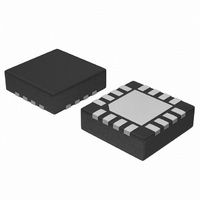
NBSG86AMNG ON Semiconductor, NBSG86AMNG Datasheet

NBSG86AMNG
Specifications of NBSG86AMNG
Available stocks
Related parts for NBSG86AMNG
NBSG86AMNG Summary of contents
Page 1
NBSG86A 2.5V/3.3V SiGe Differential Smart Gate with Output Level Select The NBSG86A is a multi-function differential Logic Gate which can be configured as an AND/NAND, OR/NOR, XOR/XNOR, or 2:1 MUX. This device is part of the GigaComm™ family of high performance ...
Page 2
A VTD1 D1 D1 SEL VTSEL SEL OLS VTD0 Figure 1. BGA-16 and LGA-16 Pinout (Top View) Table 1. Pin Description Pin BGA QFN Name I ...
Page 3
Table 2. OUTPUT LEVEL SELECT OLS OLS Q/Q VPP V 800 0.4 V 200 0.8 V 600 1 (Note 4) 400 mV EE Float 600 ...
Page 4
W VTD0 VTD0 VTD1 VTD1 VTSEL b SEL Figure 5. Configuration for OR/NOR Function 50 W VTD0 D0 ...
Page 5
Table 7. Interfacing Options INTERFACING OPTIONS CML LVDS AC-COUPLED Bias VTD0, VTD1, VTSEL and VTD0, VTD1 Inputs within (VIHCMR) Common Mode Range RSECL, PECL, NECL LVTTL, LVCMOS Table 8. ATTRIBUTES Internal Input Pulldown Resistors Internal Input Pullup Resistor ESD Protection ...
Page 6
Table 10. DC CHARACTERISTICS, INPUT WITH PECL OUTPUT Symbol Characteristic I Negative Power Supply Current EE V Output HIGH Voltage (Note 11 Output LOW Voltage (Note 11) OL (OLS = V (OLS = V CC (OLS = V ...
Page 7
Table 11. DC CHARACTERISTICS, INPUT WITH PECL OUTPUT Symbol Characteristic I Negative Power Supply Current EE V Output HIGH Voltage (Note 16 Output LOW Voltage (Note 16) OL (OLS = V (OLS = V CC (OLS = V ...
Page 8
Table 12. DC CHARACTERISTICS, NECL INPUT WITH NECL OUTPUT Symbol Characteristic I Negative Power Supply Current EE V Output HIGH Voltage (Note 21 Output LOW Voltage (Note 21) OL -3.465 -3 (OLS ...
Page 9
Table 13. AC CHARACTERISTICS for FCLGA- -3.465 V to -2.375 Symbol Characteristic f Maximum Frequency max (See Figure 8) (Note 25) V Output Voltage Amplitude OUTPP (OLS = V ...
Page 10
OLS = V 700 OLS = V OLS = FLOAT 600 500 *OLS = V 400 300 OLS = V 200 100 Figure 8. Output Voltage Amplitude (V Input Frequency (f ) for 2:1 MUX ...
Page 11
NBSG86A 300 200 100 0 -100 -200 -300 -400 -500 -600 -700 400 V - 800 OLS Figure 10. Typical OLS Input Current vs. OLS Input Voltage ( 3.3 V ...
Page 12
... Application Note AND8020/D - Termination of ECL Logic Devices.) ORDERING INFORMATION Device NBSG86ABA NBSG86ABAR2 NBSG86AMAG NBSG86AMAHTBG NBSG86AMN NBSG86AMNG NBSG86AMNR2G Board NBSG86ABAEVB †For information on tape and reel specifications, including part orientation and tape sizes, please refer to our Tape and Reel Packaging Spe‐ cifications Brochure, BRD8011/D. NBSG86A D ...
Page 13
PLASTIC (mm) BGA FLIP CHIP PACKAGE LASER MARK FOR PIN 1 IDENTIFICATION IN -X- THIS AREA D - VIEW M DETAIL K _ ...
Page 14
... SOLDERING FOOTPRINT* 1 SEATING PLANE A e/2 16X 0. *For additional information on our Pb-Free strategy and soldering details, please download the ON Semiconductor Soldering and Mounting Techniques Reference Manual, SOLDERRM/D. http://onsemi.com 14 MILLIMETERS MIN TYP MAX 0.89 0.96 1.03 0.22 0.26 0.30 0.67 0.70 0.73 ...
Page 15
... E2 e 3.25 12 0.128 *For additional information on our Pb-Free strategy and soldering details, please download the ON Semiconductor Soldering and Mounting Techniques Reference Manual, SOLDERRM/D. N. American Technical Support: 800-282-9855 Toll Free USA/Canada Europe, Middle East and Africa Technical Support: Phone: 421 33 790 2910 Japan Customer Focus Center ...


