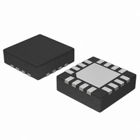
NBSG86AMNG ON Semiconductor, NBSG86AMNG Datasheet - Page 2

NBSG86AMNG
Manufacturer Part Number
NBSG86AMNG
Description
IC SMART GATE SIGE DIFF 16QFN
Manufacturer
ON Semiconductor
Specifications of NBSG86AMNG
Logic Type
Configurable Multiple Function
Number Of Circuits
2
Number Of Inputs
2
Schmitt Trigger Input
No
Output Type
Differential
Voltage - Supply
2.375 V ~ 3.465 V
Operating Temperature
-40°C ~ 85°C
Mounting Type
Surface Mount
Package / Case
16-TFQFN Exposed Pad
Product
MUX Gates
High Level Output Current
- 25 mA
Low Level Output Current
25 mA
Propagation Delay Time
0.215 ns
Supply Voltage (max)
+/- 3.465 V
Supply Voltage (min)
+/- 2.375 V
Maximum Operating Temperature
+ 85 C
Mounting Style
SMD/SMT
Minimum Operating Temperature
- 40 C
Lead Free Status / RoHS Status
Lead free / RoHS Compliant
Current - Output High, Low
-
Lead Free Status / Rohs Status
Lead free / RoHS Compliant
Other names
NBSG86AMNGOS
Available stocks
Company
Part Number
Manufacturer
Quantity
Price
Company:
Part Number:
NBSG86AMNG
Manufacturer:
ON Semiconductor
Quantity:
4
Table 1. Pin Description
1. In the differential configuration when the input termination pins (VTDx, VTDx, VTSEL) are connected to a common termination voltage,
2. All V
3. When an output level of 400 mV is desired and V
BGA
N/A
C2
C1
B1
B2
A1
A2
A3
A4
B3
B4
C4
C3
D4
D3
D2
D1
Figure 1. BGA-16 and LGA-16 Pinout (Top View)
and if no signal is applied then the device will be susceptible to self-oscillation.
Pin
CC
and V
QFN
10
12
13
14
15
16
11
C
D
A
B
1
2
3
4
5
6
7
8
9
-
EE
VTD1
VTD0
1
pins must be externally connected to Power Supply to guarantee proper operation.
SEL
SEL
(Note 3)
VTSEL
Name
VTD1
VTD1
VTD0
VTD0
OLS
SEL
SEL
V
V
D1
D1
D0
D0
EP
Q
Q
CC
EE
VTSEL
OLS
2
D1
D0
LVCMOS, LVDS,
LVCMOS, LVDS,
LVCMOS, LVDS,
LVCMOS, LVDS,
LVCMOS, LVDS,
LVCMOS, LVDS,
RSECL Output
RSECL Output
LVTTL Input
LVTTL Input
LVTTL Input
LVTTL Input
LVTTL Input
LVTTL Input
ECL, CML,
ECL, CML,
ECL, CML,
ECL, CML,
ECL, CML,
ECL, CML,
V
V
D1
D0
3
CC
EE
Input
I/O
-
-
-
-
-
-
-
-
VTD1
VTD0
4
Q
Q
CC
Input Pin for the Output Level Select (OLS). See Table 2.
Inverted Differential Select Logic Input.
Noninverted Differential Select Logic Input.
Common Internal 50 W Termination Pin for SEL/SEL. See Table 7. (Note 1)
Internal 50 W termination pin. See Table 7. (Note 1)
Noninverted Differential Input 1. Internal 75 kW to V
Inverted Differential Input 1. Internal 75 kW to V
Internal 50 W Termination Pin. See Table 7. (Note 1)
Positive Supply Voltage (Note 2)
Noninverted Differential Output. Typically Terminated with 50 W Resistor to
V
Inverted Differential Output. Typically Terminated with 50 W Resistor to
V
Negative Supply Voltage (Note 2)
Internal 50 W Termination Pin. See Table 7. (Note 1)
Inverted Differential Input 0. Internal 75 kW to V
Noninverted Differential Input 0. Internal 75 kW to V
Internal 50 W Termination Pin. See Table 7. (Note 1)
Exposed Pad. The thermally exposed pad on package bottom (see case drawing)
must be attached to a heat-sinking conduit.
- V
TT
TT
http://onsemi.com
EE
= V
= V
NBSG86A
> 3.0 V, 2 kW resistor should be connected from OLS pin to V
CC
CC
- 2 V.
- 2 V
2
VTSEL
OLS
SEL
SEL
Figure 2. QFN-16 Pinout (Top View)
1
2
3
4
VTD1
VTD0 D0
16
5
Description
NBSG86A
15
D1
6
D0 VTD0
14
D1 VTD1
7
EE
EE
and 36.5 kW to V
and 36.5 kW to V
EE
EE
13
8
.
.
12
11
10
9
V
Q
Q
V
EE
CC
CC
CC
Exposed Pad
(EP)
EE
.
.
.


