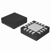
NBSG86AMNG ON Semiconductor, NBSG86AMNG Datasheet - Page 5

NBSG86AMNG
Manufacturer Part Number
NBSG86AMNG
Description
IC SMART GATE SIGE DIFF 16QFN
Manufacturer
ON Semiconductor
Specifications of NBSG86AMNG
Logic Type
Configurable Multiple Function
Number Of Circuits
2
Number Of Inputs
2
Schmitt Trigger Input
No
Output Type
Differential
Voltage - Supply
2.375 V ~ 3.465 V
Operating Temperature
-40°C ~ 85°C
Mounting Type
Surface Mount
Package / Case
16-TFQFN Exposed Pad
Product
MUX Gates
High Level Output Current
- 25 mA
Low Level Output Current
25 mA
Propagation Delay Time
0.215 ns
Supply Voltage (max)
+/- 3.465 V
Supply Voltage (min)
+/- 2.375 V
Maximum Operating Temperature
+ 85 C
Mounting Style
SMD/SMT
Minimum Operating Temperature
- 40 C
Lead Free Status / RoHS Status
Lead free / RoHS Compliant
Current - Output High, Low
-
Lead Free Status / Rohs Status
Lead free / RoHS Compliant
Other names
NBSG86AMNGOS
Available stocks
Company
Part Number
Manufacturer
Quantity
Price
Company:
Part Number:
NBSG86AMNG
Manufacturer:
ON Semiconductor
Quantity:
4
Stresses exceeding Maximum Ratings may damage the device. Maximum Ratings are stress ratings only. Functional operation above the
Recommended Operating Conditions is not implied. Extended exposure to stresses above the Recommended Operating Conditions may affect
device reliability.
7. Maximum Ratings are those values beyond which device damage may occur.
8. JEDEC standard multilayer board - 2S2P (2 signal, 2 power).
9. JEDEC standard multilayer board - 2S2P (2 signal, 2 power) with 8 filled thermal vias under exposed pad.
Table 9. MAXIMUM RATINGS
V
V
V
V
I
I
T
T
q
q
T
Symbol
IN
out
A
stg
JA
JC
sol
CC
EE
I
INPP
Table 7. Interfacing Options
INTERFACING OPTIONS
RSECL, PECL, NECL
Positive Power Supply
Negative Power Supply
Positive Input
Negative Input
Differential Input Voltage |D
Input Current Through R
Output Current
Operating Temperature Range
Storage Temperature Range
Thermal Resistance (Junction-to-Ambient)
(Note 8)
Thermal Resistance (Junction-to-Case)
Wave Solder
LVTTL, LVCMOS
AC-COUPLED
LVDS
CML
Table 8. ATTRIBUTES
6. For additional information, see Application Note AND8003/D.
Internal Input Pulldown Resistors
Internal Input Pullup Resistor
ESD Protection
Moisture Sensitivity (Note 6)
Flammability Rating
Transistor Count
Meets or exceeds JEDEC Spec EIA/JESD78 IC Latchup Test
Parameter
(Note 7)
T
Bias VTD0, VTD1, VTSEL and VTD0, VTD1 Inputs within (VIHCMR) Common Mode Range
(50 W Resistor)
n
An external voltage should be applied to the unused complementary differential input.
- D
Characteristics
n
|
Pb (BGA)
Pb-Free
Connect VTD0, VTD1, VTD0 and VTD1 together. Leave VTSEL open.
Nominal voltage 1.5 V for LVTTL and V
Connect VTD0, VTD1, VTSEL and VTD0, VTD1 to V
http://onsemi.com
V
V
V
V
V
V
Static
Surge
Continuous
Surge
16-FCBGA, FCLGA
16-QFN
0 lfpm
500 lfpm
0 lfpm
500 lfpm
2S2P (Note 8)
2S2P (Note 9)
< 15 sec
< 3 sec @ 260°C
EE
CC
EE
CC
CC
CC
FCBGA-16, FCLGA-16
Oxygen Index: 28 to 34
Charged Device Model
NBSG86A
Condition 1
= 0 V
= 0 V
= 0 V
= 0 V
- V
- V
Standard ECL Termination Techniques
Human Body Model
EE
EE
5
Machine Model
w 2.8 V
< 2.8 V
CONNECTIONS
16-QFN
(R
(R
V
V
16 FCBGA, FCLGA
16 FCBGA, FCLGA
16 QFN
16 QFN
16 FCBGA, FCLGA
16 QFN
1
2
I
I
)
)
v V
w V
Condition 2
CC
EE
CC
Pb Pkg
Level 3
Level 1
UL 94 V-0 @ 0.125 in
/2 for LVCMOS inputs.
364
37.5 kW
> 1 KV
> 4 KV
> 50 V
75 kW
Value
Pb-Free Pkg
CC
Level 3
Level 1
-65 to +150
|V
-40 to +70
-40 to +85
CC
Rating
-3.6
-3.6
41.6
35.2
108
225
265
3.6
3.6
2.8
5.0
4.0
45
80
25
50
86
- V
EE
|
Units
°C/W
°C/W
°C/W
°C/W
°C/W
°C/W
mA
mA
mA
mA
°C
°C
°C
°C
V
V
V
V
V
V


