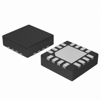
NBSG86AMNG ON Semiconductor, NBSG86AMNG Datasheet - Page 9

NBSG86AMNG
Manufacturer Part Number
NBSG86AMNG
Description
IC SMART GATE SIGE DIFF 16QFN
Manufacturer
ON Semiconductor
Specifications of NBSG86AMNG
Logic Type
Configurable Multiple Function
Number Of Circuits
2
Number Of Inputs
2
Schmitt Trigger Input
No
Output Type
Differential
Voltage - Supply
2.375 V ~ 3.465 V
Operating Temperature
-40°C ~ 85°C
Mounting Type
Surface Mount
Package / Case
16-TFQFN Exposed Pad
Product
MUX Gates
High Level Output Current
- 25 mA
Low Level Output Current
25 mA
Propagation Delay Time
0.215 ns
Supply Voltage (max)
+/- 3.465 V
Supply Voltage (min)
+/- 2.375 V
Maximum Operating Temperature
+ 85 C
Mounting Style
SMD/SMT
Minimum Operating Temperature
- 40 C
Lead Free Status / RoHS Status
Lead free / RoHS Compliant
Current - Output High, Low
-
Lead Free Status / Rohs Status
Lead free / RoHS Compliant
Other names
NBSG86AMNGOS
Available stocks
Company
Part Number
Manufacturer
Quantity
Price
Company:
Part Number:
NBSG86AMNG
Manufacturer:
ON Semiconductor
Quantity:
4
25. Measured using a 500 mV source, 50% duty cycle clock source. All loading with 50 W to V
26. t
27. V
28. Measured using a 500 mV source, 50% duty cycle clock source. All loading with 50 W to V
29. t
30. V
31. Additive RMS jitter with 50% duty cycle clock signal at 7 GHz.
32. Additive Peak-to-Peak data dependent jitter with NRZ PRBS 2
Table 13. AC CHARACTERISTICS for FCLGA-16
V
Table 14. AC CHARACTERISTICS for QFN-16
V
Symbol
Symbol
f
V
t
t
t
t
t
V
t
t
f
V
t
t
t
t
t
V
t
t
max
PLH
PHL
SKEW
SKEW
JITTER
r
f
max
PLH
PHL
SKEW
SKEW
JITTER
r
f
CC
CC
OUTPP
INPP
OUTPP
INPP
SKEW
SKEW
INPP
INPP
,
,
= 0 V; V
= 0 V; V
(max) cannot exceed V
(max) cannot exceed V
= |t
= |t
Maximum Frequency
(See Figure 8) (Note 25)
Output Voltage Amplitude
(OLS = V
Propagation Delay to Output Differential
Duty Cycle Skew (Note 26)
Channel Skew
RMS Random Clock Jitter
(See Figure 8) (Note 25)
Peak-to-Peak Data Dependent Jitter
Input Voltage Swing/Sensitivity
(Differential Configuration) (Note 27)
Output Rise/Fall Times (20% - 80%)
Maximum Frequency
(See Figure 8) (Note 28)
Output Voltage Amplitude
(OLS = V
Propagation Delay to Output Differential
Duty Cycle Skew (Note 29)
Channel Skew
RMS Random Clock Jitter
(See Figure 8) (Note 31)
Peak-to-Peak Data Dependent Jitter
(Note 32)
Input Voltage Swing/Sensitivity
(Differential Configuration) (Note 30)
Output Rise/Fall Times (20% - 80%)
PLH
PLH
EE
EE
@ 1 GHz
@ 1 GHz
= -3.465 V to -2.375 V or V
= -3.465 V to -2.375 V or V
- t
- t
PHL
PHL
CC
CC
| for a nominal 50% differential clock input waveform. See Figure 12.
| for a nominal 50% differential clock input waveform. See Figure 12.
)
)
Characteristic
Characteristic
CC
CC
- V
- V
EE
EE
.
.
CC
CC
f
f
f
f
f
f
D/SEL → Q
Q → D/SEL
D/SEL → Q
Q → D/SEL
in
in
in
in
in
in
f
= 2.375 V to 3.465 V; V
in
= 2.375 V to 3.465 V; V
v 7 Gb/s
v 7 Gb/s
v 7 GHz
v 7 GHz
v 7 GHz
v 7 GHz
= 8 GHz
(Q, Q)
(Q, Q)
t
t
http://onsemi.com
r
f
Min
550
Min
590
270
110
110
NBSG86A
75
20
75
30
17
7
7
31
-1 data rate at 7 Gb/s.
-40°C
-40°C
9
Typ
740
160
Typ
730
440
160
0.5
0.5
12
40
12
45
35
8
5
5
8
5
5
EE
EE
= 0 V
= 0 V
2600
2600
Max
Max
210
210
1.5
1.5
15
20
65
15
20
60
65
Min
500
Min
470
230
115
115
75
20
75
30
17
7
7
CC
CC
25°C
Typ
720
165
25°C
Typ
720
420
165
0.5
0.5
12
40
12
45
35
8
5
5
8
5
5
- 2.0 V. Input edge rates 40 ps (20% - 80%).
- 2.0 V. Input edge rates 40 ps (20% - 80%).
2600
2600
Max
Max
215
215
1.5
1.5
15
20
65
15
20
60
65
Min
450
120
Min
540
180
120
75
20
75
30
17
7
7
70°C
85°C
Typ
700
170
Typ
700
390
170
0.5
0.5
12
40
12
45
35
8
5
5
8
5
5
2600
2600
Max
Max
220
220
1.5
1.5
15
20
65
15
20
60
65
Unit
GHz
Unit
GHz
mV
mV
mV
mV
mV
ps
ps
ps
ps
ps
ps
ps
ps
ps
ps


