N74F373D,602 NXP Semiconductors, N74F373D,602 Datasheet - Page 2
N74F373D,602
Manufacturer Part Number
N74F373D,602
Description
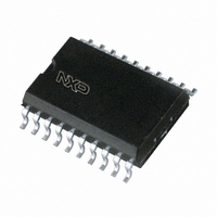
IC DTYPE LATCH OCTAL 20SOIC
Manufacturer
NXP Semiconductors
Series
74Fr
Datasheet
1.N74F374DB118.pdf
(13 pages)
Specifications of N74F373D,602
Logic Type
D-Type Transparent Latch
Package / Case
20-SOIC (7.5mm Width)
Circuit
8:8
Output Type
Tri-State
Voltage - Supply
4.5 V ~ 5.5 V
Independent Circuits
1
Delay Time - Propagation
2ns
Current - Output High, Low
3mA, 24mA
Operating Temperature
0°C ~ 70°C
Mounting Type
Surface Mount
Number Of Circuits
1
Logic Family
F
Polarity
Non-Inverting
High Level Output Current
- 3 mA
Low Level Output Current
32 mA
Propagation Delay Time
5.3 ns
Supply Voltage (max)
5.5 V
Supply Voltage (min)
4.5 V
Maximum Operating Temperature
+ 70 C
Minimum Operating Temperature
0 C
Mounting Style
SMD/SMT
Supply Current
60 mA
Lead Free Status / RoHS Status
Lead free / RoHS Compliant
Lead Free Status / RoHS Status
Lead free / RoHS Compliant, Lead free / RoHS Compliant
Other names
568-4640-5
933739560602
N74F373D
N74F373D
933739560602
N74F373D
N74F373D


The active-LOW output enable (OE) controls all eight 3-State buffers
Philips Semiconductors
FEATURES
DESCRIPTION
The 74F373 is an octal transparent latch coupled to eight 3-State
output devices. The two sections of the device are controlled
independently by enable (E) and output enable (OE) control gates.
The data on the D inputs is transferred to the latch outputs when the
enable (E) input is HIGH. The latch remains transparent to the data
input while E is HIGH, and stores the data that is present one set-up
time before the HIGH-to-LOW enable transition.
The 3-State output buffers are designed to drive heavily loaded
3-State buses, MOS memories, or MOS microprocessors.
independent of the latch operation. When OE is LOW, latched or
transparent data appears at the output.
When OE is HIGH, the outputs are in high impedance “off” state,
which means they will neither drive nor load the bus.
ORDERING INFORMATION
INPUT AND OUTPUT LOADING AND FAN OUT TABLE
NOTE: One (1.0) FAST unit load is defined as: 20 A in the HIGH state and 0.6 mA in the LOW state.
2002 Nov 20
8-bit transparent latch — 74F373
8-bit positive edge triggered register — 74F374
3-State outputs glitch free during power-up and power-down
Common 3-State output register
Independent register and 3-State buffer operation
SSOP Type II Package
Latch/flip-flop
74F373 Octal transparent latch (3-State)
74F374 Octal D-type flip-flop (3-State)
CP (74F374)
E (74F373)
20-pin plastic SSOP type II
D0 - D7
Q0 - Q7
PINS
OE
20-pin plastic SOL
20-pin plastic DIP
DESCRIPTION
Data inputs
Enable input (active-HIGH)
Output enable inputs (active-LOW)
Clock pulse input (active rising edge)
3-State outputs
V
CC
DESCRIPTION
= 5 V 10%, T
N74F373DB, N74F374DB
COMMERCIAL RANGE
N74F373N, N74F374N
N74F373D, N74F374D
ORDER CODE
amb
2
are in high impedance “off” state, which means they will neither drive
The active-LOW output enable (OE) controls all eight 3-State buffers
The 74F374 is an 8-bit edge triggered register coupled to eight
3-State output buffers. The two sections of the device are controlled
independently by clock (CP) and output enable (OE) control gates.
The register is fully edge triggered. The state of the D input, one
set-up time before the LOW-to-HIGH clock transition is transferred
to the corresponding flip-flop’s Q output.
The 3-State output buffers are designed to drive heavily loaded
3-State buses, MOS memories, or MOS microprocessors.
independent of the register operation. When OE is LOW, the data in
the register appears at the outputs. When OE is HIGH, the outputs
nor load the bus.
= 0 C to +70 C
TYPE
74F373
TYPE
74F374
HIGH / LOW
PROPAGATION
74F (U.L.)
TYPICAL f
1.0 / 1.0
1.0 / 1.0
1.0 / 1.0
1.0 / 1.0
150 / 40
TYPICAL
165 MHz
DELAY
4.5 ns
max
74F373/74F374
PKG DWG #
SOT146-1
SOT163-1
SOT339-1
TYPICAL SUPPLY
TYPICAL SUPPLY
3.0 mA / 24 mA
20 A 0.6 mA
20 A 0.6 mA
20 A 0.6 mA
20 A 0.6 mA
LOAD VALUE
HIGH/LOW
CURRENT
CURRENT
(TOTAL)
(TOTAL)
35 mA
55 mA
Product data
Related parts for N74F373D,602
Image
Part Number
Description
Manufacturer
Datasheet
Request
R

Part Number:
Description:
IC DTYPE LATCH OCTAL 20SOIC
Manufacturer:
NXP Semiconductors
Datasheet:
Part Number:
Description:
NXP Semiconductors designed the LPC2420/2460 microcontroller around a 16-bit/32-bitARM7TDMI-S CPU core with real-time debug interfaces that include both JTAG andembedded trace
Manufacturer:
NXP Semiconductors
Datasheet:

Part Number:
Description:
NXP Semiconductors designed the LPC2458 microcontroller around a 16-bit/32-bitARM7TDMI-S CPU core with real-time debug interfaces that include both JTAG andembedded trace
Manufacturer:
NXP Semiconductors
Datasheet:
Part Number:
Description:
NXP Semiconductors designed the LPC2468 microcontroller around a 16-bit/32-bitARM7TDMI-S CPU core with real-time debug interfaces that include both JTAG andembedded trace
Manufacturer:
NXP Semiconductors
Datasheet:
Part Number:
Description:
NXP Semiconductors designed the LPC2470 microcontroller, powered by theARM7TDMI-S core, to be a highly integrated microcontroller for a wide range ofapplications that require advanced communications and high quality graphic displays
Manufacturer:
NXP Semiconductors
Datasheet:
Part Number:
Description:
NXP Semiconductors designed the LPC2478 microcontroller, powered by theARM7TDMI-S core, to be a highly integrated microcontroller for a wide range ofapplications that require advanced communications and high quality graphic displays
Manufacturer:
NXP Semiconductors
Datasheet:
Part Number:
Description:
The Philips Semiconductors XA (eXtended Architecture) family of 16-bit single-chip microcontrollers is powerful enough to easily handle the requirements of high performance embedded applications, yet inexpensive enough to compete in the market for hi
Manufacturer:
NXP Semiconductors
Datasheet:
Part Number:
Description:
The XA-S3 device is a member of Philips Semiconductors? XA(eXtended Architecture) family of high performance 16-bitsingle-chip microcontrollers
Manufacturer:
NXP Semiconductors
Datasheet:

Part Number:
Description:
The NXP BlueStreak LH75401/LH75411 family consists of two low-cost 16/32-bit System-on-Chip (SoC) devices
Manufacturer:
NXP Semiconductors
Datasheet:
Part Number:
Description:
The NXP LPC3130/3131 combine an 180 MHz ARM926EJ-S CPU core, high-speed USB2
Manufacturer:
NXP Semiconductors
Datasheet:
Part Number:
Description:
The NXP LPC3141 combine a 270 MHz ARM926EJ-S CPU core, High-speed USB 2
Manufacturer:
NXP Semiconductors
Part Number:
Description:
The NXP LPC3143 combine a 270 MHz ARM926EJ-S CPU core, High-speed USB 2
Manufacturer:
NXP Semiconductors