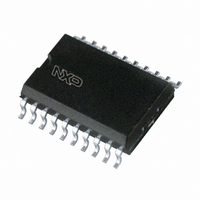
N74F373D,602 NXP Semiconductors, N74F373D,602 Datasheet - Page 6

N74F373D,602
Manufacturer Part Number
N74F373D,602
Description
IC DTYPE LATCH OCTAL 20SOIC
Manufacturer
NXP Semiconductors
Series
74Fr
Datasheet
1.N74F374DB118.pdf
(13 pages)
Specifications of N74F373D,602
Logic Type
D-Type Transparent Latch
Package / Case
20-SOIC (7.5mm Width)
Circuit
8:8
Output Type
Tri-State
Voltage - Supply
4.5 V ~ 5.5 V
Independent Circuits
1
Delay Time - Propagation
2ns
Current - Output High, Low
3mA, 24mA
Operating Temperature
0°C ~ 70°C
Mounting Type
Surface Mount
Number Of Circuits
1
Logic Family
F
Polarity
Non-Inverting
High Level Output Current
- 3 mA
Low Level Output Current
32 mA
Propagation Delay Time
5.3 ns
Supply Voltage (max)
5.5 V
Supply Voltage (min)
4.5 V
Maximum Operating Temperature
+ 70 C
Minimum Operating Temperature
0 C
Mounting Style
SMD/SMT
Supply Current
60 mA
Lead Free Status / RoHS Status
Lead free / RoHS Compliant
Lead Free Status / RoHS Status
Lead free / RoHS Compliant, Lead free / RoHS Compliant
Other names
568-4640-5
933739560602
N74F373D
N74F373D
933739560602
N74F373D
N74F373D
1. For conditions shown as MIN or MAX, use the appropriate value specified under recommended operating conditions for the applicable type.
2. All typical values are at V
3. Not more than one output should be shorted at a time. For testing I
Philips Semiconductors
DC ELECTRICAL CHARACTERISTICS
(Over recommended operating free-air temperature range unless otherwise noted.)
NOTES:
AC ELECTRICAL CHARACTERISTICS
2002 Nov 20
SYMBOL
SYMBOL
V
V
V
V
V
I
I
I
I
I
I
I
techniques are preferable in order to minimize internal heating and more accurately reflect operational values. Otherwise, prolonged shorting
I
IH
IL
OZH
OZL
OS
CC
SYMBOL
t
t
t
t
t
t
t
t
f
t
t
t
t
t
t
O
OH
O
OL
IK
PLH
PHL
PLH
PHL
PZH
PZL
PHZ
PLZ
max
PLH
PHL
PZH
PZL
PHZ
PLZ
Latch/flip-flop
of a high output may raise the chip temperature well above normal and thereby cause invalid readings in other parameter tests. In any
sequence of parameter tests, I
HIGH level output voltage
HIGH-level output voltage
LOW level output voltage
LOW-level output voltage
Input clamp voltage
Input current at maximum input voltage
High-level input current
Low-level input current
Off-state output current, high-level voltage applied
Off-state output current, low-level voltage applied
Short-circuit output current
Supply current (total)
Propagation delay
Dn to Qn
Propagation delay
E to Qn
Output enable time
to HIGH or LOW level
Output disable time
from HIGH or LOW level
Maximum clock frequency
Propagation delay
CP to Qn
Output enable time
to HIGH or LOW level
Output disable time
from HIGH or LOW level
CC
PARAMETER
= 5 V, T
OS
PARAMETER
PARAMETER
tests should be performed last.
amb
3
= 25 C.
74F373
74F374
74F373 V
74F374
CONDITION
Waveform 3
Waveform 2
Waveform 6
Waveform 7
Waveform 6
Waveform 7
Waveform 1
Waveform 1
Waveform 6
Waveform 7
Waveform 6
Waveform 7
TEST
OS
V
V
V
V
V
V
V
V
V
V
V
6
CC
CC
IH
CC
CC
IH
CC
CC
CC
CC
CC
CC
CC
CC
, the use of high-speed test apparatus and/or sample-and-hold
= MIN, I
= MIN, I
= MIN, V
= MIN, V
= MIN, I
= MAX, V
= MAX, V
= MAX, V
= MAX, V
= MAX, V
= MAX
= MAX
,
,
OH
OL
C
CONDITIONS
I
MIN
150
3.0
2.0
5.0
3.0
2.0
2.0
2.0
2.0
3.5
3.5
2.0
2.0
2.0
2.0
IL
IL
IL
IL
L
= I
I
I
I
O
O
= MAX
= MAX
= 7.0 V
= 2.7 V
= 0.5 V
= 50 pF; R
= MAX,
= MAX,
= 2.7 V
= 0.5 V
IK
TEST
T
V
amb
CC
TYP
= +5.0 V
165
= +25 C
,
,
5.3
3.7
9.0
4.0
5.0
5.6
4.5
3.8
5.0
5.0
9.0
5.3
5.3
4.3
L
1
= 500
10%V
10%V
MAX
5%V
5%V
11.5
11.0
11.0
7.0
5.0
7.0
7.5
6.5
5.0
7.5
7.5
7.5
6.0
5.5
LIMITS
CC
CC
CC
CC
C
T
L
V
amb
MIN
= 50 pF; R
74F373/74F374
–60
CC
MIN
2.4
2.7
140
3.0
2.0
5.0
3.0
2.0
2.0
2.0
2.0
3.0
3.0
2.0
2.0
2.0
2.0
= 0 C to +70 C
= +5.0 V
LIMITS
TYP
–0.73
0.35
0.35
3.4
35
57
L
2
= 500
MAX
12.0
12.0
11.5
8.0
6.0
8.0
8.5
7.0
6.0
8.5
8.5
8.5
7.0
6.5
10%
MAX
–150
0.50
0.50
–1.2
–0.6
100
–50
20
50
60
86
Product data
UNIT
UNIT
UNIT
mA
mA
mA
mA
V
V
V
V
V
ns
ns
ns
ns
ns
ns
ns
ns
A
A
A
A


