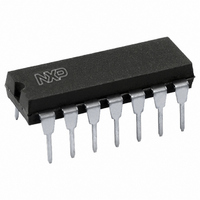
HEF4047BP,652 NXP Semiconductors, HEF4047BP,652 Datasheet - Page 13

HEF4047BP,652
Manufacturer Part Number
HEF4047BP,652
Description
IC MONO/ASTBL MULTVIBRTR 14-DIP
Manufacturer
NXP Semiconductors
Series
4000Br
Specifications of HEF4047BP,652
Logic Type
Astable, Monostable
Package / Case
14-DIP (0.300", 7.62mm)
Independent Circuits
1
Schmitt Trigger Input
No
Propagation Delay
50ns
Voltage - Supply
4.5 V ~ 15.5 V
Operating Temperature
-40°C ~ 85°C
Mounting Type
Through Hole
Elements Per Chip
1
Logic Family
HEF4000
Input Bias Current (max)
0.08 mA
Propagation Delay Time
320 ns, 130 ns, 100 ns
High Level Output Current
- 3.6 mA
Low Level Output Current
3.6 mA
Supply Voltage (max)
15 V
Supply Voltage (min)
3 V
Maximum Power Dissipation
750 mW
Maximum Operating Temperature
+ 85 C
Minimum Operating Temperature
- 40 C
Mounting Style
Through Hole
Operating Supply Voltage
3.3 V, 5 V, 9 V, 12 V
Lead Free Status / RoHS Status
Lead free / RoHS Compliant
Current - Output High, Low
-
Lead Free Status / Rohs Status
Lead free / RoHS Compliant
Other names
568-3106-5
933324240652
HEF4047BPN
933324240652
HEF4047BPN
Philips Semiconductors
5. Timing component limitations
The capacitor used in the circuit should be non-polarized and have low leakage (i.e. the parallel resistance of the
capacitor should be an order of magnitude greater than the external resistor used).
There is no upper or lower limit for either R
However, in consideration of accuracy, C
this capacitance can be measured and taken into account).
R
The recommended values for R
should be:
6. Power consumption
In the standby mode (monostable or astable), power dissipation will be a function of leakage current in the circuit.
For dynamic operation, the power needed to charge the external timing capacitor C
Because the power dissipation does not depend on R
of C
Typical power consumption in astable mode is shown in Figs 10, 11 and 12.
January 1995
Astable mode:
Monostable mode:
t
Monostable/astable multivibrator
must be much larger than the LOCMOS ‘ON’ resistance in series with it, which typically is hundreds of ohms.
t
. The value of R would depend on the desired period (within the limitations discussed previously).
C
10 k
t
100 pF, up to any practical value,
R
t
1 M .
P = 2 C
P = 4 C
P =
-------------------------------------------------------------------- - f at output pins 10 and 11
2 9 C
t
t
V
V
t
and C
2
2
f (f at output pin 13)
f (f at output pins 10 and 11)
t
V
2
t
T
to maintain agreement with previously calculated formulae without trimming
t
duty cycle
must be much larger than the inherent stray capacitance in the system (unless
t
or C
t
value to maintain oscillation.
t
, a design for minimum power dissipation would be a small value
13
t
is given by the following formulae:
Product specification
HEF4047B
MSI


