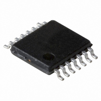
GTL2014PW,112 NXP Semiconductors, GTL2014PW,112 Datasheet

GTL2014PW,112
Specifications of GTL2014PW,112
935277499112
GTL2014PW
Related parts for GTL2014PW,112
GTL2014PW,112 Summary of contents
Page 1
GTL2014 4-bit LVTTL to GTL transceiver Rev. 01 — 19 May 2005 1. General description The GTL2014 is a 4-bit translating transceiver designed for 3.3 V LVTTL system interface with a GTL /GTL/GTL+ bus. The direction pin allows the part ...
Page 2
Philips Semiconductors 4. Ordering information Table 2: Type number GTL2014PW Standard packing quantities and other packaging data are available at www.standardics.philips.com/packaging . 4.1 Ordering options Table 3: Type number GTL2014PW 5. Functional diagram Fig 1. Logic diagram for GTL2014 9397 ...
Page 3
Philips Semiconductors 6. Pinning information 6.1 Pinning Fig 2. Pin configuration for TSSOP14 6.2 Pin description Table 4: Symbol DIR VREF GND Functional description Refer to 7.1 Function table ...
Page 4
Philips Semiconductors 8. Limiting values Table 6: In accordance with the Absolute Maximum Rating System (IEC 60134). Voltages are referenced to GND (ground = 0 V). Symbol ...
Page 5
Philips Semiconductors 9. Recommended operating conditions Table 7: Symbol Parameter ref amb [1] Unused inputs must be held HIGH or LOW to prevent them ...
Page 6
Philips Semiconductors 10. Static characteristics Table 8: Static characteristics Recommended operating conditions; voltages are referenced to GND (ground = 0 V). T Symbol Parameter V HIGH-level output OH voltage V LOW-level output OL voltage I input current I I off-state ...
Page 7
Philips Semiconductors 11. Dynamic characteristics Table 9: Dynamic characteristics V = 3 Symbol Parameter GTL ; 0.9 V ref TT t propagation delay PLH t PHL t ...
Page 8
Philips Semiconductors 11.1 Waveforms ref a. Pulse duration Fig 3. Voltage waveforms Fig 4. Propagation delay 9397 750 13534 Product data sheet 3 ...
Page 9
Philips Semiconductors 12. Test information Fig 5. Load circuitry for switching times Fig 6. Load circuit for B outputs R — Load resistor L C — Load capacitance; includes jig and probe capacitance L R — Termination resistance; should be ...
Page 10
Philips Semiconductors 13. Package outline TSSOP14: plastic thin shrink small outline package; 14 leads; body width 4 pin 1 index 1 e DIMENSIONS (mm are the original dimensions) A UNIT ...
Page 11
Philips Semiconductors 14. Soldering 14.1 Introduction to soldering surface mount packages This text gives a very brief insight to a complex technology. A more in-depth account of soldering ICs can be found in our Data Handbook IC26; Integrated Circuit Packages ...
Page 12
Philips Semiconductors – smaller than 1.27 mm, the footprint longitudinal axis must be parallel to the transport direction of the printed-circuit board. The footprint must incorporate solder thieves at the downstream end. • For packages with leads on four sides, ...
Page 13
Philips Semiconductors [4] These packages are not suitable for wave soldering. On versions with the heatsink on the bottom side, the solder cannot penetrate between the printed-circuit board and the heatsink. On versions with the heatsink on the top side, ...
Page 14
Philips Semiconductors 17. Data sheet status [1] Level Data sheet status Product status I Objective data Development II Preliminary data Qualification III Product data Production [1] Please consult the most recently issued data sheet before initiating or completing a design. ...
Page 15
Philips Semiconductors 22. Contents 1 General description . . . . . . . . . . . . . . . . . . . . . . 1 2 Features . . . . . . . . ...


