SSTUB32866EC/G,518 NXP Semiconductors, SSTUB32866EC/G,518 Datasheet - Page 10
SSTUB32866EC/G,518
Manufacturer Part Number
SSTUB32866EC/G,518
Description
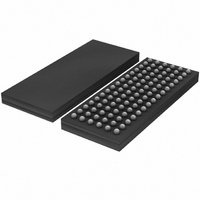
IC REG BUFFER 25BIT 96-LFBGA
Manufacturer
NXP Semiconductors
Datasheet
1.SSTUB32866ECG518.pdf
(30 pages)
Specifications of SSTUB32866EC/G,518
Logic Type
1:1, 1:2 Configurable Registered Buffer with Parity
Package / Case
96-LFBGA
Supply Voltage
1.7 V ~ 2 V
Number Of Bits
25, 14
Operating Temperature
0°C ~ 70°C
Mounting Type
Surface Mount
Logic Family
SSTU
Number Of Circuits
1
Maximum Clock Frequency
450 MHz
Propagation Delay Time
1.5 ns
High Level Output Current
- 8 mA
Low Level Output Current
8 mA
Supply Voltage (max)
2 V
Maximum Operating Temperature
+ 70 C
Minimum Operating Temperature
0 C
Mounting Style
SMD/SMT
Supply Voltage (min)
1.7 V
Lead Free Status / RoHS Status
Lead free / RoHS Compliant
Lead Free Status / RoHS Status
Lead free / RoHS Compliant, Lead free / RoHS Compliant
Other names
568-3543-2
935281279518
SSTUB32866EC/G-T
935281279518
SSTUB32866EC/G-T
Available stocks
Company
Part Number
Manufacturer
Quantity
Price
Company:

Part Number:
SSTUB32866EC/G,518
Manufacturer:
NXP Semiconductors
Quantity:
10 000


NXP Semiconductors
Table 5.
L = LOW voltage level; H = HIGH voltage level; X = don’t care;
[1]
[2]
[3]
[4]
8. Limiting values
Table 6.
In accordance with the Absolute Maximum Rating System (IEC 60134).
[1]
[2]
SSTUB32866_4
Product data sheet
Symbol
V
V
V
I
I
I
I
T
V
IK
OK
O
CCC
RESET
stg
DD
I
O
ESD
H
H
H
H
H
H
H
H
H
H
PPO
Data inputs = D2, D3, D5, D6, D8 to D25 when C0 = 0 and C1 = 0.
Data inputs = D2, D3, D5, D6, D8 to D14 when C0 = 0 and C1 = 1.
Data inputs = D1 to D6, D8 to D10, D12, D13 when C0 = 1 and C1 = 1.
PAR_IN arrives one clock cycle (C0 = 0), or two clock cycles (C0 = 1), after the data to which it applies.
This condition assumes QERR is HIGH at the crossing of CK going HIGH and CK going LOW. If QERR is LOW, it stays latched LOW for
two clock cycles or until RESET is driven LOW.
The input and output negative voltage ratings may be exceeded if the input and output clamping current ratings are observed.
This value is limited to 2.5 V maximum.
L
0
is the previous state of output PPO; QERR
Parity and standby function table
Limiting values
X or floating X or floating X or floating X or floating
Parameter
supply voltage
input voltage
output voltage
input clamping current
output clamping current
output current
continuous current through
each V
storage temperature
electrostatic discharge
voltage
DCS
H
H
H
H
H
X
L
L
L
L
DD
or GND pin
CSR
X
X
X
X
H
X
L
L
L
L
Conditions
receiver
driver
V
V
continuous; 0 V < V
Human Body Model (HBM); 1.5 kΩ; 100 pF
Machine Model (MM); 0 Ω; 200 pF
All information provided in this document is subject to legal disclaimers.
I
O
L or H
< 0 V or V
CK
< 0 V or V
↑
↑
↑
↑
↑
↑
↑
↑
↑
Inputs
0
is the previous state of output QERR.
Rev. 04 — 15 April 2010
I
O
> V
1.8 V DDR2-800 configurable registered buffer with parity
> V
L or H
DD
CK
↓
↓
↓
↓
↓
↓
↓
↓
↓
DD
O
↑
< V
= LOW to HIGH transition;
DD
∑ of inputs = H
X or floating
(D1 to D25)
even
even
even
even
odd
odd
odd
odd
X
X
X or floating
PAR_IN
↓
H
H
H
H
X
X
Min
−0.5
−0.5
−0.5
-
-
-
-
−65
2
200
L
L
L
L
SSTUB32866
= HIGH to LOW transition.
[2]
[1]
[1]
PPO
PPO
PPO
Max
+2.5
+2.5
V
−50
±50
±50
±100
+150
-
-
© NXP B.V. 2010. All rights reserved.
DD
H
H
H
H
L
L
L
L
L
Outputs
[3]
[2]
+ 0.5
0
0
[2]
QERR
QERR
QERR
[1]
10 of 30
H
H
H
H
H
L
L
L
L
Unit
V
V
V
mA
mA
mA
mA
°C
kV
V
[4]
0
0
Related parts for SSTUB32866EC/G,518
Image
Part Number
Description
Manufacturer
Datasheet
Request
R

Part Number:
Description:
NXP Semiconductors designed the LPC2420/2460 microcontroller around a 16-bit/32-bitARM7TDMI-S CPU core with real-time debug interfaces that include both JTAG andembedded trace
Manufacturer:
NXP Semiconductors
Datasheet:

Part Number:
Description:
NXP Semiconductors designed the LPC2458 microcontroller around a 16-bit/32-bitARM7TDMI-S CPU core with real-time debug interfaces that include both JTAG andembedded trace
Manufacturer:
NXP Semiconductors
Datasheet:
Part Number:
Description:
NXP Semiconductors designed the LPC2468 microcontroller around a 16-bit/32-bitARM7TDMI-S CPU core with real-time debug interfaces that include both JTAG andembedded trace
Manufacturer:
NXP Semiconductors
Datasheet:
Part Number:
Description:
NXP Semiconductors designed the LPC2470 microcontroller, powered by theARM7TDMI-S core, to be a highly integrated microcontroller for a wide range ofapplications that require advanced communications and high quality graphic displays
Manufacturer:
NXP Semiconductors
Datasheet:
Part Number:
Description:
NXP Semiconductors designed the LPC2478 microcontroller, powered by theARM7TDMI-S core, to be a highly integrated microcontroller for a wide range ofapplications that require advanced communications and high quality graphic displays
Manufacturer:
NXP Semiconductors
Datasheet:
Part Number:
Description:
The Philips Semiconductors XA (eXtended Architecture) family of 16-bit single-chip microcontrollers is powerful enough to easily handle the requirements of high performance embedded applications, yet inexpensive enough to compete in the market for hi
Manufacturer:
NXP Semiconductors
Datasheet:
Part Number:
Description:
The XA-S3 device is a member of Philips Semiconductors? XA(eXtended Architecture) family of high performance 16-bitsingle-chip microcontrollers
Manufacturer:
NXP Semiconductors
Datasheet:

Part Number:
Description:
The NXP BlueStreak LH75401/LH75411 family consists of two low-cost 16/32-bit System-on-Chip (SoC) devices
Manufacturer:
NXP Semiconductors
Datasheet:
Part Number:
Description:
The NXP LPC3130/3131 combine an 180 MHz ARM926EJ-S CPU core, high-speed USB2
Manufacturer:
NXP Semiconductors
Datasheet:
Part Number:
Description:
The NXP LPC3141 combine a 270 MHz ARM926EJ-S CPU core, High-speed USB 2
Manufacturer:
NXP Semiconductors
Part Number:
Description:
The NXP LPC3143 combine a 270 MHz ARM926EJ-S CPU core, High-speed USB 2
Manufacturer:
NXP Semiconductors

Part Number:
Description:
The NXP LPC3152 combines an 180 MHz ARM926EJ-S CPU core, High-speed USB 2
Manufacturer:
NXP Semiconductors
Part Number:
Description:
The NXP LPC3154 combines an 180 MHz ARM926EJ-S CPU core, High-speed USB 2
Manufacturer:
NXP Semiconductors

Part Number:
Description:
Standard level N-channel enhancement mode Field-Effect Transistor (FET) in a plastic package using NXP High-Performance Automotive (HPA) TrenchMOS technology
Manufacturer:
NXP Semiconductors
Datasheet: