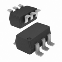
74AVCH1T45GW,125 NXP Semiconductors, 74AVCH1T45GW,125 Datasheet - Page 16

74AVCH1T45GW,125
Manufacturer Part Number
74AVCH1T45GW,125
Description
IC TRANSCVR TRI-ST DL SPLY SC88
Manufacturer
NXP Semiconductors
Series
74AVCHr
Datasheet
1.74AVCH1T45GW125.pdf
(22 pages)
Specifications of 74AVCH1T45GW,125
Output Type
Logic
Package / Case
SC-70-6, SC-88, SOT-363
Logic Function
Translator, Bidirectional, 3-State
Number Of Bits
2
Input Type
Logic
Number Of Channels
2
Number Of Outputs/channel
1
Differential - Input:output
No/No
Propagation Delay (max)
2.7ns
Voltage - Supply
0.8 V ~ 3.6 V
Operating Temperature
-40°C ~ 125°C
Supply Voltage
0.8 V ~ 3.6 V
Logic Family
AVC
Number Of Channels Per Chip
1
Input Level
CMOS
Output Level
CMOS
High Level Output Current
- 12 mA
Low Level Output Current
12 mA
Supply Voltage (max)
3.6 V
Supply Voltage (min)
0.8 V
Maximum Operating Temperature
+ 125 C
Function
Bus Transceiver with Voltage Translation
Input Bias Current (max)
24 uA
Minimum Operating Temperature
- 40 C
Mounting Style
SMD/SMT
Polarity
Non-Inverting
Logic Type
CMOS
Number Of Circuits
1
Data Rate
-
Lead Free Status / RoHS Status
Lead free / RoHS Compliant
Data Rate
-
Lead Free Status / Rohs Status
Lead free / RoHS Compliant
Other names
74AVCH1T45GW-G
74AVCH1T45GW-G
935284156125
74AVCH1T45GW-G
935284156125
NXP Semiconductors
74AVCH1T45_2
Product data sheet
13.2 Bidirectional logic level-shifting application
Figure 9
application. Since the device does not have an output enable pin, the system designer
should take precautions to avoid bus contention between system-1 and system-2 when
changing directions.
Table 16
and then from system-2 to system-1.
Table 16.
[1]
State DIR CTRL I/O-1
1
2
3
4
Fig 9.
H = HIGH voltage level;
L = LOW voltage level;
Z = high-impedance OFF-state.
H
H
L
L
shows the 74AVCH1T45 being used in a bidirectional logic level-shifting
gives a sequence that will illustrate data transmission from system-1 to system-2
Bidirectional logic level-shifting application
Description bidirectional logic level-shifting application
DIR CTRL
VCC1
I/O-1
system-1
output
Z
Z
input
VCC1
Rev. 02 — 5 May 2009
I/O-2
input
Z
Z
output
V
CC(A)
GND
A
1
2
3
Description
system-1 data to system-2
system-2 is getting ready to send data to system-1.
I/O-1 and I/O-2 are disabled. The bus-line state
depends on bus hold.
DIR bit is set LOW. I/O-1 and I/O-2 still are disabled.
The bus-line state depends on bus hold.
system-2 data to system-1
74AVCH1T45
Dual supply translating transceiver; 3-state
6
5
4
V
DIR
B
CC(B)
74AVCH1T45
VCC2
[1]
system-2
VCC2
I/O-2
001aag890
© NXP B.V. 2009. All rights reserved.
16 of 22


