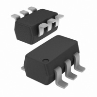
74AVCH1T45GW,125 NXP Semiconductors, 74AVCH1T45GW,125 Datasheet - Page 4

74AVCH1T45GW,125
Manufacturer Part Number
74AVCH1T45GW,125
Description
IC TRANSCVR TRI-ST DL SPLY SC88
Manufacturer
NXP Semiconductors
Series
74AVCHr
Datasheet
1.74AVCH1T45GW125.pdf
(22 pages)
Specifications of 74AVCH1T45GW,125
Output Type
Logic
Package / Case
SC-70-6, SC-88, SOT-363
Logic Function
Translator, Bidirectional, 3-State
Number Of Bits
2
Input Type
Logic
Number Of Channels
2
Number Of Outputs/channel
1
Differential - Input:output
No/No
Propagation Delay (max)
2.7ns
Voltage - Supply
0.8 V ~ 3.6 V
Operating Temperature
-40°C ~ 125°C
Supply Voltage
0.8 V ~ 3.6 V
Logic Family
AVC
Number Of Channels Per Chip
1
Input Level
CMOS
Output Level
CMOS
High Level Output Current
- 12 mA
Low Level Output Current
12 mA
Supply Voltage (max)
3.6 V
Supply Voltage (min)
0.8 V
Maximum Operating Temperature
+ 125 C
Function
Bus Transceiver with Voltage Translation
Input Bias Current (max)
24 uA
Minimum Operating Temperature
- 40 C
Mounting Style
SMD/SMT
Polarity
Non-Inverting
Logic Type
CMOS
Number Of Circuits
1
Data Rate
-
Lead Free Status / RoHS Status
Lead free / RoHS Compliant
Data Rate
-
Lead Free Status / Rohs Status
Lead free / RoHS Compliant
Other names
74AVCH1T45GW-G
74AVCH1T45GW-G
935284156125
74AVCH1T45GW-G
935284156125
NXP Semiconductors
8. Limiting values
Table 5.
In accordance with the Absolute Maximum Rating System (IEC 60134). Voltages are referenced to GND (ground = 0 V).
[1]
[2]
[3]
[4]
9. Recommended operating conditions
Table 6.
[1]
[2]
74AVCH1T45_2
Product data sheet
Symbol
V
V
I
V
I
V
I
I
I
T
P
Symbol
V
V
V
V
T
IK
OK
O
CC
GND
stg
amb
t/ V
CC(A)
CC(B)
I
O
tot
CC(A)
CC(B)
I
O
The minimum input voltage ratings and output voltage ratings may be exceeded if the input and output current ratings are observed.
V
V
For SC-88 packages: above 87.5 C the value of P
For XSON6 packages: above 118 C the value of P
V
V
CCO
CCO
CCO
CCI
is the supply voltage associated with the input port.
is the supply voltage associated with the output port.
+ 0.5 V should not exceed 4.6 V.
is the supply voltage associated with the output port.
Limiting values
Recommended operating conditions
Parameter
supply voltage A
supply voltage B
input clamping current
input voltage
output clamping current
output voltage
output current
supply current
ground current
storage temperature
total power dissipation
Parameter
supply voltage A
supply voltage B
input voltage
output voltage
ambient temperature
input transition rise and fall rate
Conditions
V
V
Active mode
Suspend or 3-state mode
V
I
T
CC(A)
amb
I
O
O
< 0 V
< 0 V
= 0 V to V
tot
Conditions
Active mode
Suspend or 3-state mode
V
= 40 C to +125 C
tot
or I
CCI
derates linearly with 4.0 mW/K.
Rev. 02 — 5 May 2009
derates linearly with 7.8 mW/K.
CC(B)
= 0.8 V to 3.6 V
CCO
Dual supply translating transceiver; 3-state
[1][2][3]
[1]
[1]
[4]
[1]
[2]
Min
-
-
-
0.5
0.5
50
0.5
50
0.5
0.5
100
65
Min
0.8
0.8
0
0
0
-
40
74AVCH1T45
Max
+4.6
+4.6
-
+4.6
-
V
+4.6
100
-
+150
250
Max
3.6
3.6
3.6
V
3.6
+125
5
50
CCO
CCO
© NXP B.V. 2009. All rights reserved.
+ 0.5
Unit
V
V
mA
V
mA
V
V
mA
mA
mA
mW
Unit
V
V
V
V
V
ns/V
C
C
4 of 22


