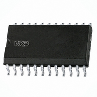
74LVC4245AD,112 NXP Semiconductors, 74LVC4245AD,112 Datasheet - Page 4

74LVC4245AD,112
Manufacturer Part Number
74LVC4245AD,112
Description
IC TRANSCVR TRI-ST DL 24SOIC
Manufacturer
NXP Semiconductors
Series
74LVCr
Datasheet
1.74LVC4245APW112.pdf
(17 pages)
Specifications of 74LVC4245AD,112
Logic Function
Translator, 3-State
Number Of Bits
8
Input Type
TTL
Output Type
TTL
Number Of Channels
8
Number Of Outputs/channel
1
Differential - Input:output
No/No
Propagation Delay (max)
8ns
Voltage - Supply
1.5 V ~ 5.5 V
Operating Temperature
-40°C ~ 125°C
Package / Case
24-SOIC (7.5mm Width)
Supply Voltage
1.5 V ~ 5.5 V
Logic Family
74LVC
Propagation Delay Time
10 ns
Maximum Operating Temperature
125 C
Maximum Power Dissipation
500 mW
Minimum Operating Temperature
- 40 C
Mounting Style
SMD/SMT
Logic Type
Standard Transceivers
Lead Free Status / RoHS Status
Lead free / RoHS Compliant
Data Rate
-
Lead Free Status / Rohs Status
Lead free / RoHS Compliant
Other names
568-1585-5
74LVC4245AD
935260749112
74LVC4245AD
935260749112
NXP Semiconductors
6. Functional description
Table 3.
[1]
7. Limiting values
Table 4.
In accordance with the Absolute Maximum Rating System (IEC 60134). Voltages are referenced to GND (ground = 0 V).
[1]
[2]
8. Recommended operating conditions
Table 5.
74LVC4245A_6
Product data sheet
Input
OE
L
L
H
Symbol
V
V
I
V
I
V
I
I
I
T
P
Symbol
V
V
V
V
T
IK
OK
O
CC
GND
stg
amb
CCA
CCB
I
O
tot
CCA
CCB
I
O
H = HIGH voltage level; L = LOW voltage level; X = don’t care; Z = high-impedance OFF-state.
The input and output voltage ratings may be exceeded if the input and output current ratings are observed.
For SO24 packages: above 70 C the value of P
For (T)SSOP24 packages: above 60 C the value of P
For DHVQFN24 packages: above 60 C the value of P
Functional table
Limiting values
Recommended operating conditions
Parameter
supply voltage 5 V port (for maximum
speed performance)
supply voltage 3 V port (for low-voltage
applications)
input voltage
output voltage
ambient temperature
Parameter
supply voltage 5 V port
supply voltage 3 V port
input clamping current
input voltage
output clamping current
output voltage
output current
supply current
ground current
storage temperature
power dissipation
[1]
DIR
L
H
X
tot
Conditions
V
V
output HIGH or LOW state
output 3-state
V
T
amb
I
O
O
derates linearly with 8 mW/K.
Rev. 06 — 18 January 2008
< 0 V
> V
= 0 V to V
tot
tot
= 40 C to +125 C
Conditions
V
V
for control inputs
output HIGH or LOW state
output 3-state
CC
derates linearly with 5.5 mW/K.
CCA
CCA
derates linearly with 4.5 mW/K.
or V
V
V
CC
O
CCB
CCB
Input/output
An
A = B
input
Z
< 0 V
; see
; see
Octal dual supply translating transceiver; 3-state
Figure 5
Figure 5
[1]
[1]
[1]
[2]
Min
1.5
1.5
0
0
0
Min
-
-
-
-
40
0.5
0.5
50
0.5
0.5
0.5
100
65
Bn
input
B = A
Z
74LVC4245A
Typ
-
-
-
-
-
-
Max
+6.5
+4.6
-
+6.5
V
+6.5
100
-
+150
500
50
50
CC
© NXP B.V. 2008. All rights reserved.
+ 0.5
Max
5.5
3.6
5.5
V
5.5
+125
CC
Unit
V
V
mA
V
mA
V
V
mA
mA
mA
mW
C
Unit
V
V
V
V
V
C
4 of 17


