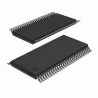
74ALVCH16501DGG,11 NXP Semiconductors, 74ALVCH16501DGG,11 Datasheet - Page 5

74ALVCH16501DGG,11
Manufacturer Part Number
74ALVCH16501DGG,11
Description
IC UNIV BUS TXRX 18BIT 56TSSOP
Manufacturer
NXP Semiconductors
Series
74ALVCHr
Datasheet
1.74ALVCH16501DGG11.pdf
(18 pages)
Specifications of 74ALVCH16501DGG,11
Logic Type
Universal Bus Transceiver
Number Of Circuits
18-Bit
Current - Output High, Low
24mA, 24mA
Voltage - Supply
2.3 V ~ 3.6 V
Operating Temperature
-40°C ~ 85°C
Mounting Type
Surface Mount
Package / Case
56-TSSOP
Lead Free Status / RoHS Status
Lead free / RoHS Compliant
Other names
74ALVCH16501DG-T
74ALVCH16501DG-T
935262543118
74ALVCH16501DG-T
935262543118
NXP Semiconductors
Table 2.
6. Functional description
Table 3.
[1]
7. Limiting values
Table 4.
In accordance with the Absolute Maximum Rating System (IEC 60134). Voltages are referenced to GND (ground = 0 V).
74ALVCH16501_3
Product data sheet
Symbol
CPBA
B0 to B17
CPAB
Inputs
OEAB
L
H
H
H
H
H
H
H
H
Symbol
V
I
V
I
V
I
I
IK
OK
O
CC
CC
I
O
A-to-B data flow is shown; B-to-A flow is similar but uses OEBA, LEBA and CPBA.
H = HIGH voltage level;
h = HIGH voltage level one set-up time prior to the enable or clock transition;
L = LOW voltage level;
l = LOW voltage level one set-up time prior to the enable or clock transition;
X = don’t care;
Z = high-impedance OFF-state;
↓
↑ = LOW-to-HIGH clock transition.
= HIGH-to-LOW clock transition;
Pin description
Function table
Limiting values
Parameter
supply voltage
input clamping current
input voltage
output clamping current
output voltage
output current
supply current
LEAB
X
H
H
↓
↓
L
L
L
L
6.1 Function table
Pin
30
54, 52, 51, 49, 48, 47, 45, 44, 43, 42, 41, 40, 38, 37, 36, 34, 33, 31
55
[1]
…continued
CPAB
X
X
X
X
X
↑
↑
H or L
H or L
Conditions
V
control inputs
data inputs
V
V
All information provided in this document is subject to legal disclaimers.
I
O
O
< 0 V
> V
= 0 V to V
An
X
H
L
h
l
h
l
X
X
CC
Rev. 03 — 2 April 2010
or V
CC
O
< 0 V
Output
Bn
Z
H
L
H
L
H
L
H
L
18-bit universal bus transceiver; 3-state
Operating mode
disabled
transparent
latch data and display
clock data and display
hold data and display
[1]
[1]
[1]
74ALVCH16501
Description
clock input B-to-A
data inputs or outputs
clock input A-to-B
Min
−0.5
−50
−0.5
−0.5
-
−0.5
-
-
Max
+4.6
-
+4.6
V
±50
V
±50
100
CC
CC
© NXP B.V. 2010. All rights reserved.
+ 0.5
+ 0.5
Unit
V
mA
V
V
mA
V
mA
mA
5 of 18


