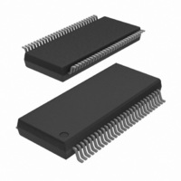
74ALVT16601DL,512 NXP Semiconductors, 74ALVT16601DL,512 Datasheet - Page 10

74ALVT16601DL,512
Manufacturer Part Number
74ALVT16601DL,512
Description
IC 18BIT UNVRSL BUS TXRX 56SSOP
Manufacturer
NXP Semiconductors
Series
74ALVTr
Datasheet
1.74ALVT16601DGG118.pdf
(20 pages)
Specifications of 74ALVT16601DL,512
Logic Type
Universal Bus Transceiver
Number Of Circuits
18-Bit
Current - Output High, Low
8mA, 24mA; 32mA, 64mA
Voltage - Supply
2.3 V ~ 2.7 V, 3 V ~ 3.6 V
Operating Temperature
-40°C ~ 85°C
Mounting Type
Surface Mount
Package / Case
56-SSOP
Lead Free Status / RoHS Status
Lead free / RoHS Compliant
Other names
74ALVT16601DL
74ALVT16601DL
935219470512
74ALVT16601DL
935219470512
Philips Semiconductors
Table 7:
At recommended operating conditions; voltages are referenced to GND (ground = 0 V).
T
[1]
[2]
[3]
[4]
[5]
[6]
[7]
[8]
[9]
[10] This parameter is valid for any V
74ALVT16601_3
Product data sheet
Symbol Parameter
V
V
I
I
I
I
I
I
C
C
LI
OFF
HOLD
EX
PU
CC
amb
I
OL
RST
i
io
CC
, I
All typical values are at V
For valid test results, data must not be loaded into the flip-flops (or latches) after applying power.
Unused pins at V
Not guaranteed.
This parameter is valid for any V
a transition time of 100 s is permitted. This parameter is valid for T
I
This is the increase in supply current for each input at the specified voltage level other than V
All typical values are at V
This is the bus hold overdrive current required to force the input to the opposite logic state.
a transition time of 100 s is permitted. This parameter is valid for T
CC
= 40 C to +85 C .
PD
is measured with outputs pulled up to V
LOW-level output voltage
power-up LOW-state output voltage V
input leakage current
power-down leakage current
bus hold current data inputs
external current into output
power-up/down 3-state output
current
supply current
additional supply current per input
pin
input capacitance of control pins
input/output capacitance of I/O pins V
Static characteristics
control pins
I/O data pins
CC
or GND.
CC
CC
= 2.5 V and T
= 3.3 V and T
CC
CC
…continued
between 0 V and 1.2 V with a transition time of up to 10 ms. From V
between 0 V and 1.2 V with a transition time of up to 10 ms. From V
amb
amb
CC
= 25 C.
= 25 C.
or pulled down to ground.
Conditions
V
V
V
V
V
V
V
V
V
V
V
V
V
V
output in HIGH-state when V
V
V
V
don’t care
V
V
V
V
V
CC
CC
CC
CC
CC
I
CC
CC
CC
CC
CC
CC
CC
CC
CC
O
CC
I
CC
CC
CC
CC
I
I/O
outputs HIGH-state
outputs LOW-state
outputs disabled
= V
= GND or V
= 0 V or V
= 5.5 V; V
= 0 V or V
= 3.0 V; I
= 3.0 V; I
= 3.0 V; I
= 3.0 V; I
= 2.7 V; I
= 3.6 V; V
= 0 V or 3.6 V; V
= 3.6 V; V
= 3.6 V; V
= 3.6 V; V
= 0 V; V
= 3 V; V
= 3 V; V
= 0 V to 3.6 V; V
= 3.6 V; V
= 3 V to 3.6 V; one input at
or GND
Rev. 03 — 5 July 2005
CC
1.2 V; V
0.6 V, other inputs at
or GND
I
I
I
CC
CC
OL
OL
OL
OL
O
or V
= 0.8 V
= 2.0 V
O
CC
I
I
I
I
I
CC
= 1 mA;
= V
= 5.5 V
= V
= 0 V
= GND or V
= 2.3 V
= 0.5 V to V
= 100 A
= 16 mA
= 32 mA
= 64 mA
; OEAB or OEAB
; outputs disabled
amb
amb
O
CC
CC
= 0 V to 4.5 V
= 25 C only.
= 25 C only.
I
CC
= 5.5 V
or GND
= 3.6 V
CC
CC
O
; I
18-bit universal bus transceiver; 3-state
;
> V
O
= 0 A
CC
;
CC
[10]
[2]
[3]
[3]
[3]
[9]
[9]
[9]
[6]
[7]
or GND.
© Koninklijke Philips Electronics N.V. 2005. All rights reserved.
74ALVT16601
Min
-
-
-
-
-
-
-
-
-
-
-
75
-
-
-
-
-
-
75
500
CC
CC
= 1.2 V to V
= 1.2 V to V
Typ
0.07
0.25
0.3
0.4
-
0.1
0.1
0.1
0.5
+0.1
0.1
130
-
10
1
0.06
3.5
0.06
0.04
4
8
140
CC
CC
Max
0.2
0.4
0.5
0.55
0.55
10
20
10
-
-
-
125
0.1
5
0.1
0.4
-
-
1
5
100
100
= 2.5 V
= 3.3 V
Unit
V
V
V
V
V
mA
mA
mA
mA
pF
pF
10 of 20
A
A
A
A
A
A
A
A
A
A
A
0.2 V
0.3 V


