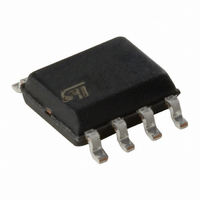
M95256-WMN6P STMicroelectronics, M95256-WMN6P Datasheet - Page 13

M95256-WMN6P
Manufacturer Part Number
M95256-WMN6P
Description
IC EEPROM 256KBIT 5MHZ 8SOIC
Manufacturer
STMicroelectronics
Specifications of M95256-WMN6P
Format - Memory
EEPROMs - Serial
Memory Type
EEPROM
Memory Size
256K (32K x 8)
Speed
5MHz
Interface
SPI, 3-Wire Serial
Voltage - Supply
2.5 V ~ 5.5 V
Operating Temperature
-40°C ~ 85°C
Package / Case
8-SOIC (3.9mm Width)
Organization
32 K x 8
Interface Type
SPI
Maximum Clock Frequency
5 MHz
Access Time
60 ns
Supply Voltage (max)
6.5 V
Supply Voltage (min)
2.5 V
Maximum Operating Current
5 mA
Maximum Operating Temperature
+ 130 C
Mounting Style
SMD/SMT
Minimum Operating Temperature
- 40 C
Operating Supply Voltage
2.5 V, 5.5 V
Memory Configuration
32K X 8
Ic Interface Type
Serial, SPI
Clock Frequency
20MHz
Supply Voltage Range
2.5V To 5.5V
Memory Case Style
SOIC
No. Of Pins
8
Rohs Compliant
Yes
Lead Free Status / RoHS Status
Lead free / RoHS Compliant
Other names
497-6357-5
M95256-WMN6P
M95256-WMN6P
Available stocks
Company
Part Number
Manufacturer
Quantity
Price
M95256-DR, M95256, M95256-W, M95256-R
4.2
4.3
Status Register
Figure 4
Status Register contains a number of status and control bits that can be read or set (as
appropriate) by specific instructions. For a detailed description of the Status Register bits,
see
Data protection and protocol control
Non-volatile memory devices can be used in environments that are particularly noisy, and
within applications that could experience problems if memory bytes are corrupted.
Consequently, the device features the following data protection mechanisms:
●
●
●
●
For any instruction to be accepted, and executed, Chip Select (S) must be driven high after
the rising edge of Serial Clock (C) for the last bit of the instruction, and before the next rising
edge of Serial Clock (C).
Two points need to be noted in the previous sentence:
●
●
Table 2.
Section 5.3: Read Status Register
Write and Write Status Register instructions are checked that they consist of a number
of clock pulses that is a multiple of eight, before they are accepted for execution.
All instructions that modify data must be preceded by a Write Enable (WREN)
instruction to set the Write Enable Latch (WEL) bit. This bit is returned to its reset state
by the following events:
–
–
–
–
The Block Protect (BP1, BP0) bits in the Status Register allow part of the memory to be
configured as read-only.
The Write Protect (W) signal is used to protect the Block Protect (BP1, BP0) bits of the
Status Register.
The ‘last bit of the instruction’ can be the eighth bit of the instruction code, or the eighth
bit of a data byte, depending on the instruction (except for Read Status Register
(RDSR) and Read (READ) instructions).
The ‘next rising edge of Serial Clock (C)’ might (or might not) be the next bus
transaction for some other device on the SPI bus.
BP1
Status Register bits
0
0
1
1
shows the position of the Status Register in the control logic of the device. The
Power-up
Write Disable (WRDI) instruction completion
Write Status Register (WRSR) instruction completion
Write (WRITE) instruction completion
Write-protected block size
BP0
0
1
0
1
Doc ID 12276 Rev 11
Protected block
Whole memory
Upper quarter
Upper half
(RDSR).
none
M95256, M95256-W, M95256-R
Protected array addresse
6000h - 7FFFh
4000h - 7FFFh
0000h - 7FFFh
none
Operating features
13/48


