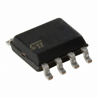
M95256-WMN6P STMicroelectronics, M95256-WMN6P Datasheet - Page 18

M95256-WMN6P
Manufacturer Part Number
M95256-WMN6P
Description
IC EEPROM 256KBIT 5MHZ 8SOIC
Manufacturer
STMicroelectronics
Specifications of M95256-WMN6P
Format - Memory
EEPROMs - Serial
Memory Type
EEPROM
Memory Size
256K (32K x 8)
Speed
5MHz
Interface
SPI, 3-Wire Serial
Voltage - Supply
2.5 V ~ 5.5 V
Operating Temperature
-40°C ~ 85°C
Package / Case
8-SOIC (3.9mm Width)
Organization
32 K x 8
Interface Type
SPI
Maximum Clock Frequency
5 MHz
Access Time
60 ns
Supply Voltage (max)
6.5 V
Supply Voltage (min)
2.5 V
Maximum Operating Current
5 mA
Maximum Operating Temperature
+ 130 C
Mounting Style
SMD/SMT
Minimum Operating Temperature
- 40 C
Operating Supply Voltage
2.5 V, 5.5 V
Memory Configuration
32K X 8
Ic Interface Type
Serial, SPI
Clock Frequency
20MHz
Supply Voltage Range
2.5V To 5.5V
Memory Case Style
SOIC
No. Of Pins
8
Rohs Compliant
Yes
Lead Free Status / RoHS Status
Lead free / RoHS Compliant
Other names
497-6357-5
M95256-WMN6P
M95256-WMN6P
Available stocks
Company
Part Number
Manufacturer
Quantity
Price
Instructions
5.4
18/48
Write Status Register (WRSR)
The Write Status Register (WRSR) instruction allows new values to be written to the Status
Register. Before it can be accepted, a Write Enable (WREN) instruction must have been
previously executed.
The Write Status Register (WRSR) instruction is entered by driving Chip Select (S) Low,
followed by the instruction code, the data byte on Serial Data Input (D) and the Chip Select
(S) driven High. Chip Select (S) must be driven High after the rising edge of Serial Clock (C)
that latches in the eighth bit of the data byte, and before the next rising edge of Serial Clock
(C). Otherwise, the Write Status Register (WRSR) instruction is not properly executed.
The instruction sequence is shown in
Driving the Select (S) High at a byte boundary of the input data triggers the self timed Write
cycle, and continues for a period t
Table
be read to check the value of the Write In Progress (WIP) bit: the WIP bit is 1 during the self-
timed Write cycle t
Latch) is also reset when the Write cycle t
The Write Status Register (WRSR) instruction allows the user to change the values of the
BP1, BP0 bits and the SRWD bit:
●
●
The contents of the SRWD and BP1, BP0 bits are updated after the completion of the
WRSR instruction, including the t
The Write Status Register (WRSR) instruction has no effect on bits b6, b5, b4, b1, b0 of the
Status Register. Bits b6, b5, b4 are always read as 0.
Table 6.
1. As defined by the values in the Block Protect (BP1, BP0) bits of the Status Register, as shown in
W signal
1
0
1
0
The Block Protect (BP1, BP0) bits define the size of the area that is to be treated as
read only, as defined in
The SRWD bit (Status Register Write Disable bit), in accordance with the signal read
on the Write Protect pin (W), allows the user to set or reset the Write protection mode
of the Status Register itself, as defined in
Write Status Register (WRSR) instruction is not executed.
20). While the Write Status Register cycle is in progress, the Status Register may still
SRWD
Protection modes
bit
0
0
1
1
W
Protected
Hardware
Protected
, and is 0 when the Write cycle is completed. The WEL bit (Write Enable
Software
(HPM)
(SPM)
Mode
Table
Doc ID 12276 Rev 11
Write protection of the
Status Register is
Writable (if the WREN
instruction has set the
WEL bit)
The values in the BP1
and BP0 bits can be
changed
Status Register is
Hardware write
protected
The values in the BP1
and BP0 bits cannot be
changed
W
Status Register
W
2.
Write cycle.
(as specified in
Figure
W
is completed.
9.
M95256-DR, M95256, M95256-W, M95256-R
Table 6
Table
Write-protected
Write-protected
Protected area
When in Write Protected mode, the
17,
Table
Memory content
(1)
18,
Ready to accept Write
instructions
Ready to accept Write
instructions
Table 19
Unprotected area
and
Table
6.
(1)


