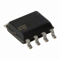
M95256-WMN6P STMicroelectronics, M95256-WMN6P Datasheet - Page 27

M95256-WMN6P
Manufacturer Part Number
M95256-WMN6P
Description
IC EEPROM 256KBIT 5MHZ 8SOIC
Manufacturer
STMicroelectronics
Specifications of M95256-WMN6P
Format - Memory
EEPROMs - Serial
Memory Type
EEPROM
Memory Size
256K (32K x 8)
Speed
5MHz
Interface
SPI, 3-Wire Serial
Voltage - Supply
2.5 V ~ 5.5 V
Operating Temperature
-40°C ~ 85°C
Package / Case
8-SOIC (3.9mm Width)
Organization
32 K x 8
Interface Type
SPI
Maximum Clock Frequency
5 MHz
Access Time
60 ns
Supply Voltage (max)
6.5 V
Supply Voltage (min)
2.5 V
Maximum Operating Current
5 mA
Maximum Operating Temperature
+ 130 C
Mounting Style
SMD/SMT
Minimum Operating Temperature
- 40 C
Operating Supply Voltage
2.5 V, 5.5 V
Memory Configuration
32K X 8
Ic Interface Type
Serial, SPI
Clock Frequency
20MHz
Supply Voltage Range
2.5V To 5.5V
Memory Case Style
SOIC
No. Of Pins
8
Rohs Compliant
Yes
Lead Free Status / RoHS Status
Lead free / RoHS Compliant
Other names
497-6357-5
M95256-WMN6P
M95256-WMN6P
Available stocks
Company
Part Number
Manufacturer
Quantity
Price
M95256-DR, M95256, M95256-W, M95256-R
6
7
Delivery state
The device is delivered with the memory array set at all 1s (FFh). The Status Register Write
Disable (SRWD) and Block Protect (BP1 and BP0) bits are initialized to 0.
Connecting to the SPI bus
These devices are fully compatible with the SPI protocol.
All instructions, addresses and input data bytes are shifted in to the device, most significant
bit first. The Serial Data input (D) is sampled on the first rising edge of the Serial Clock (C)
after Chip Select (S) goes low.
All output data bytes are shifted out of the device, most significant bit first. The Serial Data
output (Q) is latched on the first falling edge of the Serial Clock (C) after the instruction (such
as the Read from Memory Array and Read Status Register instructions) have been clocked
into the device.
Figure 17
bus. Only one memory device is selected at a time, so only one memory device drives the
Serial Data output (Q) line at a time, the other memory devices are high impedance.
Figure 17. Bus master and memory devices on the SPI bus
1. The Write Protect (W) and Hold (HOLD) signals should be driven, high or low as appropriate.
The pull-up resistor R (represented in
bus master leaves the S line in the high-impedance state.
In applications where the bus master might enter a state where all SPI bus inputs/outputs
would be in high impedance at the same time (for example, if the bus master is reset during
CS3
SPI Interface with
(ST6, ST7, ST9,
(CPOL, CPHA) =
ST10, Others)
(0, 0) or (1, 1)
Bus Master
CS2 CS1
shows an example of three memory devices connected to an MCU, on an SPI
SDO
SDI
SCK
R
R
Doc ID 12276 Rev 11
C Q D
S
SPI Memory
Device
W
Figure
V
CC
HOLD
V
17) ensures that a device is not selected if the
SS
R
C Q D
S
SPI Memory
Device
W
V
CC
HOLD
V
SS
R
C Q D
S
SPI Memory
Device
Delivery state
W
V
CC
HOLD
AI12304b
V
V
V
27/48
SS
CC
SS


