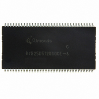
HYB25D512800CE-6 Qimonda, HYB25D512800CE-6 Datasheet - Page 21

HYB25D512800CE-6
Manufacturer Part Number
HYB25D512800CE-6
Description
IC DDR SDRAM 512MBIT 66TSOP
Manufacturer
Qimonda
Datasheet
1.HYB25D512800CE-6.pdf
(42 pages)
Specifications of HYB25D512800CE-6
Format - Memory
RAM
Memory Type
DDR SDRAM
Memory Size
512M (64M x 8)
Speed
166MHz
Interface
Parallel
Voltage - Supply
2.3 V ~ 2.7 V
Operating Temperature
0°C ~ 70°C
Package / Case
66-TSOP
Lead Free Status / RoHS Status
Lead free / RoHS Compliant
Other names
675-1008-2
Available stocks
Company
Part Number
Manufacturer
Quantity
Price
Part Number:
HYB25D512800CE-6
Manufacturer:
QIMONDA
Quantity:
20 000
4
The truth tables in this chapter summarize the commands and there signal coding to control a standard Double-Data-Rate
SDRAM.
1) CKE is HIGH for all commands shown exceptSelf Refresh.
2) Deselect and NOP are functionally interchangeable.
3) BA0, BA1 provide bank address and A0 - Ai provide row address.
4) BA0, BA1 provide bank address; A0 - Ai provide column address ; A10 HIGH enables the Auto Precharge feature (nonpersistent), A10
5) Applies only to read bursts with Auto Precharge disabled; this command is undefined (and should not be used) for read bursts with Auto
6) A10 LOW: BA0, BA1 determine which bank is precharged. A10 HIGH: all banks are precharged and BA0, BA1 are “Don’t Care”.
7) This command is AUTO REFRESH if CKE is HIGH; Self Refresh if CKE is LOW
8) Internal refresh counter controls row and bank addressing; all inputs and I/Os are “Don’t Care” except for CKE.
9) BA0, BA1 select either the Base or the Extended Mode Register (BA0 = 0, BA1 = 0 selects Mode Register; BA0 = 1, BA1 = 0 selects
1) Used to mask write data; provided coincident with the corresponding data.
Rev. 1.41, 2007-12
03292006-3TFJ-HNV3
Name (Function)
Deselect (NOP)
No Operation (NOP)
Active (Select Bank And Activate Row)
Read (Select Bank And Column, And Start Read Burst)
Write (Select Bank And Column, And Start Write Burst)
Burst Terminate
Precharge (Deactivate Row In Bank Or Banks)
Auto Refresh Or Self Refresh (Enter Self Refresh Mode)
Mode Register Set
Name (Function)
Write Enable
Write Inhibit
LOW disables the Auto Precharge feature.
Precharge enabled or for write bursts.
Extended Mode Register; other combinations of BA0-BA1 are reserved; A0 - Ai provide the op-code to be written to the selected Mode
Register.
Truth Tables
Date: 2007-12-13
V
REF
must be maintained during Self Refresh operation.
21
L
CS
H
L
L
L
L
L
L
L
RAS
X
H
L
H
H
H
L
L
L
H
L
H
CAS
X
H
L
H
L
L
HY[B/I]25D512[40/80/16]0C[C/E/F/T](L)
512-Mbit Double-Data-Rate SDRAM
L
WE Address
X
H
H
H
L
L
H
L
Truth Table 2: DM Operation
X
X
Bank/Row
Bank/Col
Bank/Col
X
Code
Op-Code
X
Truth Table 1: Commands
DM
L
H
Internet Data Sheet
DQs
Valid
X
MNE
NOP
NOP
ACT
Read
Write
BST
PRE
AR/SR
MRS
TABLE 13
TABLE 14
Note
1)
Note
1)2)
1)2)
1)3)
1)4)
1)4)
1)5)
1)6)
1)7)8)
1)9)


