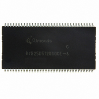
HYB25D512800CE-6 Qimonda, HYB25D512800CE-6 Datasheet - Page 24

HYB25D512800CE-6
Manufacturer Part Number
HYB25D512800CE-6
Description
IC DDR SDRAM 512MBIT 66TSOP
Manufacturer
Qimonda
Datasheet
1.HYB25D512800CE-6.pdf
(42 pages)
Specifications of HYB25D512800CE-6
Format - Memory
RAM
Memory Type
DDR SDRAM
Memory Size
512M (64M x 8)
Speed
166MHz
Interface
Parallel
Voltage - Supply
2.3 V ~ 2.7 V
Operating Temperature
0°C ~ 70°C
Package / Case
66-TSOP
Lead Free Status / RoHS Status
Lead free / RoHS Compliant
Other names
675-1008-2
Available stocks
Company
Part Number
Manufacturer
Quantity
Price
Part Number:
HYB25D512800CE-6
Manufacturer:
QIMONDA
Quantity:
20 000
1) This table applies when CKE n-1 was HIGH and CKE n is HIGH (see
2) This table describes alternate bank operation, except where noted, i.e., the current state is for bank n and the commands shown are those
3) Current state definitions: Idle: The bank has been precharged, and
4) AUTO REFRESH and Mode Register Set commands may only be issued when all banks are idle.
5) A BURST TERMINATE command cannot be issued to another bank; it applies to the bank represented by the current state only.
6) All states and sequences not shown are illegal or reserved.
7) Reads or Writes listed in the Command/Action column include Reads or Writes with Auto Precharge enabled and Reads or Writes with
8) Requires appropriate DM masking.
9) Concurrent Auto Precharge:This device supports “Concurrent Auto Precharge”. When a read with auto precharge or a write with auto
Rev. 1.41, 2007-12
03292006-3TFJ-HNV3
Current State
Any
Idle
Row
Activating,
Active, or
Precharging
Read (Auto
Precharge
Disabled)
Write (Auto
Precharge
Disabled)
Read (With
Auto
Precharge)
Write (With
Auto
Precharge)
if the previous state was self refresh)
allowed to be issued to bank m (assuming that bank m is in such a state that the given command is allowable). Exceptions are covered in
the notes below.
and
Auto Precharge disabled, and has not yet terminated or been terminated. Write: A Write burst has been initiated, with Auto Precharge
disabled, and has not yet terminated or been terminated.
Auto Precharge disabled.
precharge is enabled any command may follow to the other banks as long as that command does not interrupt the read or write data
t
RCD
has been met. No data bursts/accesses and no register accesses are in progress. Read: A Read burst has been initiated, with
CS
H
L
X
L
L
L
L
L
L
L
L
L
L
L
L
L
L
L
L
L
L
L
RAS CAS WE Command
X
H
X
L
H
H
L
L
H
L
L
H
H
L
L
H
H
L
L
H
H
L
X
H
X
H
L
L
H
H
L
H
H
L
L
H
H
L
L
H
H
L
L
H
Truth Table 5: Current State Bank n - Command to Bank m (different bank)
X
H
X
H
H
L
L
H
H
L
H
H
L
L
H
H
L
L
H
H
L
L
Deselect
No Operation
Any Command
Otherwise Allowed to
Bank m
Active
Read
Write
Precharge
Active
Read
Precharge
Active
Read
Write
Precharge
Active
Read
Write
Precharge
Active
Read
Write
Precharge
Date: 2007-12-13
24
t
RP
Table
has been met. Row Active: A row in the bank has been activated,
Action
NOP. Continue previous operation.
NOP. Continue previous operation.
–
Select and activate row
Select column and start Read burst
Select column and start Write burst
–
Select and activate row
Select column and start new Read burst
–
Select and activate row
Select column and start Read burst
Select column and start new Write burst
–
Select and activate row
Select column and start new Read burst
Select column and start Write burst
–
Select and activate row
Select column and start Read burst
Select column and start new Write burst
–
15: Clock Enable (CKE) and after
HY[B/I]25D512[40/80/16]0C[C/E/F/T](L)
512-Mbit Double-Data-Rate SDRAM
t
XSNR
Internet Data Sheet
/
t
XSRD
TABLE 17
Notes
1)2)3)4)5)6)
1)2)3)4)5)6)
1)2)3)4)5)6)
1)2)3)4)5)6)
1)2)3)4)5)6)7)
1)2)3)4)5)6)7)
1)2)3)4)5)6)
1)2)3)4)5)6)
1)2)3)4)5)6)7)
1)2)3)4)5)6)
1)2)3)4)5)6)
1)2)3)4)5)6)7)8)
1)2)3)4)5)6)7)
1)2)3)4)5)6)
1)2)3)4)5)6)
1)2)3)4)5)6)7)9)
1)2)3)4)5)6)7)9)10)
1)2)3)4)5)6)
1)2)3)4)5)6)
1)2)3)4)5)6)7)9)
1)2)3)4)5)6)7)9)
1)2)3)4)5)6)
has been met,


