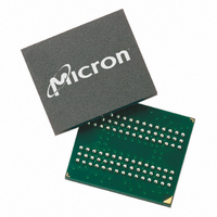
MT46H16M16LFBF-6 IT:A Micron Technology Inc, MT46H16M16LFBF-6 IT:A Datasheet - Page 33

MT46H16M16LFBF-6 IT:A
Manufacturer Part Number
MT46H16M16LFBF-6 IT:A
Description
IC DDR SDRAM 256MBIT 60VFBGA
Manufacturer
Micron Technology Inc
Type
DDR SDRAMr
Specifications of MT46H16M16LFBF-6 IT:A
Format - Memory
RAM
Memory Type
Mobile DDR SDRAM
Memory Size
256M (16Mx16)
Speed
166MHz
Interface
Parallel
Voltage - Supply
1.7 V ~ 1.95 V
Operating Temperature
-40°C ~ 85°C
Package / Case
60-VFBGA
Organization
16Mx16
Density
256Mb
Address Bus
15b
Access Time (max)
6.5/5ns
Maximum Clock Rate
166MHz
Operating Supply Voltage (typ)
1.8V
Package Type
VFBGA
Operating Temp Range
-40C to 85C
Operating Supply Voltage (max)
1.95V
Operating Supply Voltage (min)
1.7V
Supply Current
100mA
Pin Count
60
Mounting
Surface Mount
Operating Temperature Classification
Industrial
Lead Free Status / Rohs Status
Compliant
Other names
Q3368612
Truncated READs
Figure 18:
PDF: 09005aef82091978 / Source: 09005aef8209195b
MT46H16M16LF__2.fm - Rev. H 6/08 EN
Command
Command
Address
Address
Terminating a READ Burst
DQS
DQS
CK#
CK#
DQ
DQ
CK
CK
Notes:
Note:
Bank a ,
Bank a ,
READ
READ
Col n
Col n
T0
T0
Data from any non-auto precharge READ burst may be truncated with a BURST TERMI-
NATE command, as shown in Figure 18. The BURST TERMINATE latency is equal to the
READ (CAS) latency; for example, the BURST TERMINATE command should be issued x
cycles after the READ command, where x equals the number of desired data element
pairs (pairs are required by the 2n-prefetch architecture).
Data from any non-auto precharge READ burst must be completed or truncated before a
subsequent WRITE command can be issued. If truncation is necessary, the BURST
TERMINATE command must be used, as shown in Figure 18. The
shown; the
[MAX] are defined in the section on WRITEs.)
A READ burst may be followed by, or truncated with, a PRECHARGE command to the
same bank provided that auto precharge was not activated. The PRECHARGE command
should be issued x cycles after the READ command, where x equals the number of
desired data element pairs (pairs are required by the n-prefetch architecture). This is
shown in Figure 20 on page 35. Following the PRECHARGE command, a subsequent
command to the same bank cannot be issued until
1. D
2. BL = 4 or 8.
3. Shown with nominal
4. BST = BURST TERMINATE command; page remains open.
Part of the row precharge time is hidden during the access of the last data elements.
OUT
CL = 2
n = data-out from column n.
t
BST
BST
DQSS (MAX) case has a longer bus idle time. (
T1
T1
CL = 3
4
4
T1n
t
D
AC,
OUT
n
T2
NOP
NOP
T2
t
DQSCK, and
33
D
n+1
T2n
OUT
T2n
D
OUT
n
T3
T3
NOP
NOP
Micron Technology, Inc., reserves the right to change products or specifications without notice.
t
256Mb: x16, x32 Mobile DDR SDRAM
Transitioning data
DQSQ.
D
n+1
T3n
OUT
t
T4
T4
NOP
NOP
RP is met.
t
DQSS [MIN] and
©2005 Micron Technology, Inc. All rights reserved.
T5
T5
NOP
Don’t Care
NOP
t
DQSS (MIN) case is
Operations
t
DQSS


