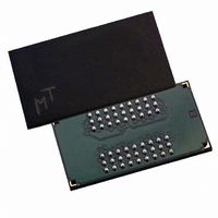
MT48LC8M16LFB4-8 IT:G Micron Technology Inc, MT48LC8M16LFB4-8 IT:G Datasheet - Page 37

MT48LC8M16LFB4-8 IT:G
Manufacturer Part Number
MT48LC8M16LFB4-8 IT:G
Description
IC SDRAM 128MBIT 125MHZ 54VFBGA
Manufacturer
Micron Technology Inc
Type
Mobile SDRAMr
Specifications of MT48LC8M16LFB4-8 IT:G
Format - Memory
RAM
Memory Type
Mobile SDRAM
Memory Size
128M (8Mx16)
Speed
125MHz
Interface
Parallel
Voltage - Supply
3 V ~ 3.6 V
Operating Temperature
-40°C ~ 85°C
Package / Case
54-VFBGA
Organization
8Mx16
Density
128Mb
Address Bus
14b
Access Time (max)
19/8/7ns
Maximum Clock Rate
125MHz
Operating Supply Voltage (typ)
3.3V
Package Type
VFBGA
Operating Temp Range
-40C to 85C
Operating Supply Voltage (max)
3.6V
Operating Supply Voltage (min)
3V
Supply Current
100mA
Pin Count
54
Mounting
Surface Mount
Operating Temperature Classification
Industrial
Lead Free Status / RoHS Status
Lead free / RoHS Compliant
Figure 23:
Figure 24:
PDF: 09005aef807f4885/Source: 09005aef8071a76b
128Mbx16x32Mobile_2.fm - Rev. M 1/09 EN
Random WRITE Cycles
WRITE-to-READ
Notes:
Notes:
In the case of a fixed-length burst being executed to completion, a PRECHARGE
command issued at the optimum time (as described above) provides the same operation
that would result from the same fixed-length burst with auto precharge. The disadvan-
tage of the PRECHARGE command is that it requires that the command and address
buses be available at the appropriate time to issue the command; the advantage of the
PRECHARGE command is that it can be used to truncate fixed-length or full-page bursts.
COMMAND
1. Each WRITE command may be to any bank.
2. DQM is LOW.
3. Example shows BL = 1 or an interrupting BL > 1.
COMMAND
1. The WRITE command may be to any bank, and the READ command may be to any bank.
2. DQM is LOW.
3. CL = 2 for illustration.
4. Data n + 1 is either the last data of BL = 1 or the last desired of a longer burst.
ADDRESS
ADDRESS
CLK
DQ
CLK
DQ
WRITE
BANK,
TRANSITIONING DATA
COL n
D
T0
BANK,
WRITE
COL n
n
IN
D
T0
n
IN
n + 1
NOP
T1
D
WRITE
BANK,
COL a
IN
T1
D
a
IN
TRANSITIONING DATA
BANK,
READ
COL b
T2
WRITE
BANK,
COL x
D
T2
37
x
IN
DON’T CARE
T3
NOP
WRITE
BANK,
COL m
T3
D
m
IN
Micron Technology, Inc., reserves the right to change products or specifications without notice.
NOP
D
T4
OUT
b
128Mb: x16, x32 Mobile SDRAM
DON’T CARE
NOP
T5
b + 1
D
OUT
©2001 Micron Technology, Inc. All rights reserved.
READs


