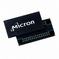
MT47H64M8CB-5E:B Micron Technology Inc, MT47H64M8CB-5E:B Datasheet - Page 36

MT47H64M8CB-5E:B
Manufacturer Part Number
MT47H64M8CB-5E:B
Description
IC DDR2 SDRAM 512MBIT 5NS 60FBGA
Manufacturer
Micron Technology Inc
Datasheet
1.MT47H64M8CB-5EB.pdf
(133 pages)
Specifications of MT47H64M8CB-5E:B
Format - Memory
RAM
Memory Type
DDR2 SDRAM
Memory Size
512M (64M x 8)
Speed
5ns
Interface
Parallel
Voltage - Supply
1.7 V ~ 1.9 V
Operating Temperature
0°C ~ 85°C
Package / Case
60-FBGA
Lead Free Status / RoHS Status
Lead free / RoHS Compliant
Available stocks
Company
Part Number
Manufacturer
Quantity
Price
Company:
Part Number:
MT47H64M8CB-5E:B
Manufacturer:
MICRON
Quantity:
12 388
Company:
Part Number:
MT47H64M8CB-5E:B
Manufacturer:
Micron Technology Inc
Quantity:
10 000
Company:
Part Number:
MT47H64M8CB-5E:B TR
Manufacturer:
Micron Technology Inc
Quantity:
10 000
READs
READ Command
READ Operation
PDF: 09005aef8117c18e, Source: 09005aef8211b2e6
512MbDDR2_2.fm - Rev. K 8/06 EN
The READ command is used to initiate a burst read access to an active row. The value on
the BA1–BA0 inputs selects the bank, and the address provided on inputs A0–i (where i =
A9 for x16, A9 for x8, or A9, A11 for x4) selects the starting column location. The value on
input A10 determines whether or not auto precharge is used. If auto precharge is
selected, the row being accessed will be precharged at the end of the READ burst; if auto
precharge is not selected, the row will remain open for subsequent accesses.
READ bursts are initiated with a READ command, as shown in Figure 16 on page 37. The
starting column and bank addresses are provided with the READ command and auto
precharge is either enabled or disabled for that burst access. If auto precharge is
enabled, the row being accessed is automatically precharged at the completion of the
burst. If auto precharge is disabled, the row will be left open after the completion of the
burst.
During READ bursts, the valid data-out element from the starting column address will
be available READ latency (RL) clocks later. RL is defined as the sum of AL and CL;
RL = AL + CL. The value for AL and CL are programmable via the MR and EMR
commands, respectively. Each subsequent data-out element will be valid nominally at
the next positive or negative clock edge (i.e., at the next crossing of CK and CK#).
Figure 18 on page 38 shows examples of RL based on different AL and CL settings.
DQS/DQS# is driven by the DDR2 SDRAM along with output data. The initial LOW state
on DQS and HIGH state on DQS# is known as the read preamble (
on DQS and HIGH state on DQS# coincident with the last data-out element is known as
the read postamble (
Upon completion of a burst, assuming no other commands have been initiated, the DQ
will go High-Z. A detailed explanation of
window hold), and the valid data window are depicted in Figure 27 on page 46 and
Figure 28 on page 47. A detailed explanation of
t
Data from any READ burst may be concatenated with data from a subsequent READ
command to provide a continuous flow of data. The first data element from the new
burst follows the last element of a completed burst. The new READ command should be
issued x cycles after the first READ command, where x equals BL / 2 cycles. This is shown
in Figure 19 on page 39.
AC (data-out transition skew to CK) is shown in Figure 29 on page 48.
t
RPST).
36
Micron Technology, Inc., reserves the right to change products or specifications without notice.
t
DQSQ (valid data-out skew),
512Mb: x4, x8, x16 DDR2 SDRAM
t
DQSCK (DQS transition skew to CK) and
©2004 Micron Technology, Inc. All rights reserved.
t
RPRE). The LOW state
t
QH (data-out
READs


