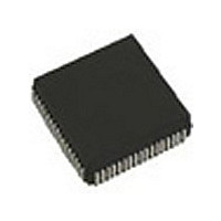
CY7C138-25JC Cypress Semiconductor Corp, CY7C138-25JC Datasheet - Page 4

CY7C138-25JC
Manufacturer Part Number
CY7C138-25JC
Description
IC SRAM 32KBIT 25NS 68PLCC
Manufacturer
Cypress Semiconductor Corp
Specifications of CY7C138-25JC
Format - Memory
RAM
Memory Type
SRAM - Dual Port, Asynchronous
Memory Size
32K (4K x 8)
Speed
25ns
Interface
Parallel
Voltage - Supply
4.5 V ~ 5.5 V
Operating Temperature
0°C ~ 70°C
Package / Case
68-PLCC
Density
32Kb
Access Time (max)
25ns
Sync/async
Asynchronous
Architecture
Not Required
Clock Freq (max)
Not RequiredMHz
Operating Supply Voltage (typ)
5V
Address Bus
12b
Package Type
PLCC
Operating Temp Range
0C to 70C
Number Of Ports
2
Supply Current
180mA
Operating Supply Voltage (min)
4.5V
Operating Supply Voltage (max)
5.5V
Operating Temperature Classification
Commercial
Mounting
Surface Mount
Pin Count
68
Word Size
8b
Number Of Words
4K
Lead Free Status / RoHS Status
Contains lead / RoHS non-compliant
Other names
428-1445
Available stocks
Company
Part Number
Manufacturer
Quantity
Price
Company:
Part Number:
CY7C138-25JC
Manufacturer:
CYPRESS
Quantity:
13 888
Company:
Part Number:
CY7C138-25JC
Manufacturer:
Cypress Semiconductor Corp
Quantity:
10 000
AC Test Loads and Waveforms
Note:
]
Electrical Characteristics
Capacitance
OUTPUT
V
V
V
V
I
I
I
I
I
I
I
Parameter
C
C
7.
OUTPUT
IX
OZ
CC
SB1
SB2
SB3
SB4
OH
OL
IH
IL
IN
OUT
C = 30 pF
Tested initially and after any design or process changes that may affect these parameters.
(a) Normal Load (Load 1)
Parameter
Load (Load 2)
Output HIGH Voltage
Output LOW Voltage
Input LOW Voltage
Input Leakage Current
Output Leakage Current
Operating Current
Standby Current
(Both Ports TTL Levels)
Standby Current
(One Port TTL Level)
Standby Current
(Both Ports CMOS Levels)
Standby Current
(One Port CMOS Level)
[7]
C = 30 pF
Description
5V
R1=893
R2=347
C138-6
Input Capacitance
Output Capacitance
C138-3
Over the Operating Range (continued)
Description
GND
3.0V
< 3 ns
V
V
GND < V
Output Disabled, GND < V
V
I
Outputs Disabled
CE
f = f
CE
f = f
Both Ports
CE and CE
V
or V
One Port
CE
V
V
Port Outputs, f = f
OUT
OUTPUT
IN
IN
IN
CC
CC
CC
L
L
L
10%
> V
> V
< 0.2V, Active
IN
MAX
MAX
= Max.,
or CE
= 0 mA,
= Min., I
= Min., I
and CE
and CE
C=30pF
(b) Thé venin Equivalent ( Load 1)
< 0.2V, f = 0
CC
CC
[6]
[6]
I
– 0.2V
R
– 0.2V or
< V
R
Test Conditions
ALL INPUT PULSES
> V
> V
90%
R
R
OH
OL
T
V
CC
> V
> V
CC
A
CC
CC
MAX
R
= 4.0 mA
= 25 C, f = 1 MHz,
= –4.0 mA
[6]
TH
– 0.2V,
IH
IH
= 5.0V
4
– 0.2V,
,
,
[6]
=250
Test Conditions
O
< V
Com’l
Ind
Com’l
Ind
Com’l
Ind
Com’l
Ind
Com’l
Ind
V
90%
TH
CC
10%
=1.4V
< 3 ns
C138-4
C138-7
Min.
–10
–10
2.4
2.2
OUTPUT
7C138-35
7C139-35
C = 5 pF
Max.
+10
+10
160
180
100
100
110
0.4
0.8
30
40
15
30
90
(c) Three-State Delay (Load 3)
Max.
10
15
Min.
–10
–10
2.4
2.2
7C138-55
7C139-55
CY7C138
CY7C139
5V
Max.
+10
+10
160
180
100
100
110
0.4
0.8
30
40
15
30
90
R1=893
R2=347
Unit
pF
pF
C138-5
Unit
mA
mA
mA
mA
mA
V
V
V
V
A
A


