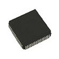
CY7C138-25JC Cypress Semiconductor Corp, CY7C138-25JC Datasheet

CY7C138-25JC
Specifications of CY7C138-25JC
Available stocks
Related parts for CY7C138-25JC
CY7C138-25JC Summary of contents
Page 1
... Document #: 38-06037 Rev 8/9 Dual-Port Static RAM Functional Description The CY7C138 and CY7C139 are high speed CMOS and dual-port static RAMs. Various arbitration schemes are included on the CY7C138/9 to handle situations when multiple processors access the same piece of data. Two ports are provided permitting independent, asynchronous access for reads and writes to any location in memory ...
Page 2
... FFE and is cleared when L left port reads location FFE. INT R cleared when right port reads location FFF. Busy Flag Master or Slave Select Power Ground 7C138-15 7C138-25 7C139-15 7C139- Commercial 220 180 Commercial 60 40 CY7C138, CY7C139 INT 54 ...
Page 3
... < 0.2V One Port Commercial > V – 0.2V Industrial V > V – 0. < 0.2V, Active IN [7] Port Outputs MAX CY7C138, CY7C139 Ambient V CC Temperature ° ° + ± 10% ° ° – + ± 10% 7C138-15 7C138-25 7C139-15 7C139-25 Unit Min Max Min Max 2.4 2 ...
Page 4
... CE > V – 0.2V Industrial V > V – 0. < 0.2V, Active IN [7] Port Outputs MAX Test Conditions T = 25° MHz 5.0V CC CY7C138, CY7C139 7C138-35 7C138-55 7C139-35 7C139-55 Unit Min Max Min Max 2.4 2.4 V 0.4 0.4 V 2.2 2.2 V 0.8 0.8 V μA –10 +10 – ...
Page 5
... C = 30pF V = 1.4V TH (b) Thé venin Equivalent ( Load 1) ALL INPUT PULSES 3.0V 90% 90% 10% 10% GND < < [9] 7C138-15 7C138-25 7C139-15 7C139-25 Min Max Min Max CY7C138, CY7C139 893Ω OUTPUT 347Ω (c) Three-State Delay (Load 3) 7C138-35 7C138-55 7C139-35 7C139-55 Min Max Min Max ...
Page 6
... Min Max Min Max Note 15 Note less than t and t is less than t HZCE LZCE HZOE – t (actual – t (actual). WDD PWE DDD SD CY7C138, CY7C139 7C138-35 7C138-55 7C139-35 7C139-55 Min Max Min Max Note 15 Note [16, 17] DATA VALID . LZOE Page Unit ...
Page 7
... Address valid prior to or coincident with CE transition LOW. 19 SEM = H when accessing RAM SEM = L when accessing semaphores. L Document #: 38-06037 Rev ACE t DOE DATA VALID t WC MATCH t PWE t SD VALID MATCH t WDD CY7C138, CY7C139 [16, 18, 19] t HZCE t HZOE t PD [20, 21 DDD VALID Page [+] Feedback ...
Page 8
... R/W must be HIGH during all address transitions. Document #: 38-06037 Rev SCE PWE t SD DATA VALID HIGH IMPEDANCE SCE PWE DATA VALID t HZWE HIGH IMPEDANCE allow the I/O drivers to turn off and data to be PWE HZWE SD CY7C138, CY7C139 [22, 23, 24 LZOE [22, 24, 25 LZWE Page [+] Feedback ...
Page 9
... CE = HIGH for the duration of the above timing (both write and read cycle). Document #: 38-06037 Rev VALID ADDRESS SCE SOP t SD DATA VALID PWE t SWRD t SOP READ CYCLE MATCH t SPS MATCH CY7C138, CY7C139 [26] t OHA t ACE DATA VALID OUT t DOE [27, 28, 29] Page [+] Feedback ...
Page 10
... SPS Document #: 38-06037 Rev MATCH t PWE t SD VALID MATCH t BLA t WDD t PWE HIGH L CY7C138, CY7C139 [21 BHA t BDD t DDD VALID Page [+] Feedback ...
Page 11
... BUSY will be asserted. PS Document #: 38-06037 Rev. *E ADDRESS MATCH BLC ADDRESS MATCH BLC ADDRESS MISMATCH t t BLA BHA ADDRESS MISMATCH t t BLA BHA CY7C138, CY7C139 [30] t BHC t BHC [30] Page [+] Feedback ...
Page 12
... 32 depends on which enable pin (CE or R/W INS INR L Document #: 38-06037 Rev. *E Figure 14. Interrupt Timing Diagrams t WC WRITE FFF t [31] HA [32] t INR t WC WRITE FFE t [31] HA [32] t INR ) is asserted last. L CY7C138, CY7C139 t RC READ FFF t RC READ FFE Page [+] Feedback ...
Page 13
... Architecture The CY7C138/9 consists of an array of 4K words of 8/9 bits each of dual-port RAM cells, I/O and address lines, and control signals (CE, OE, R/W). These control pins permit independent access for reads or writes to any location in memory. To handle simulta- neous writes and reads to the same location, a BUSY pin is provided on each port. Two interrupt (INT) pins can be used for port– ...
Page 14
... L X FFF I/O Left I/O Right 0-7/8 0-7 CY7C138, CY7C139 Operation Right Port INT R 0- FFE FFF Status Semaphore free Left port obtains semaphore Right side is denied access Right port is granted access to semaphore No change. Left port is denied access Left port obtains semaphore ...
Page 15
... TYPICAL ACCESS TIME CHANGE vs. OUTPUT LOADING 30.0 25.0 20.0 15.0 10 4. 25° 200 400 600 800 1000 CAPACITANCE (pF) CY7C138, CY7C139 OUTPUT SOURCE CURRENT vs. OUTPUT VOLTAGE 200 160 120 25° 125 0 1.0 2.0 3.0 4.0 OUTPUT VOLTAGE (V) OUTPUT SINK CURRENT vs ...
Page 16
... Ordering Information 4K x8 Dual-Port SRAM Speed Ordering Code (ns) 15 CY7C138-15JC CY7C138-15JXC 25 CY7C138-25JC CY7C138-25JXC CY7C138-25JI CY7C138-25JXI 35 CY7C138-35JC CY7C138-35JI 55 CY7C138-55JC CY7C138-55JI Package Diagram Figure 16. 68-Pin Plastic Leaded Chip Carrier (51-85005) Document #: 38-06037 Rev. *E Package Package Type Diagram 51-85005 68-Pin Plastic Leaded Chip Carrier ...
Page 17
... Document History Page Document Title: CY7C138, CY7C139 4K x 8/9 Dual-Port Static RAM with Sem, Int, Busy Document Number: 38-06037 Orig. of Rev. ECN No. Change ** 110180 SZV *A 122287 RBI *B 393403 YIM *C 2623658 VKN/PYRS *D 2672737 GNKK *E 2714768 VKN/AESA Sales, Solutions, and Legal Information Worldwide Sales and Design Support Cypress maintains a worldwide network of offices, solution centers, manufacturer’ ...


