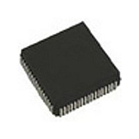
CY7C138-25JC Cypress Semiconductor Corp, CY7C138-25JC Datasheet - Page 5

CY7C138-25JC
Manufacturer Part Number
CY7C138-25JC
Description
IC SRAM 32KBIT 25NS 68PLCC
Manufacturer
Cypress Semiconductor Corp
Specifications of CY7C138-25JC
Format - Memory
RAM
Memory Type
SRAM - Dual Port, Asynchronous
Memory Size
32K (4K x 8)
Speed
25ns
Interface
Parallel
Voltage - Supply
4.5 V ~ 5.5 V
Operating Temperature
0°C ~ 70°C
Package / Case
68-PLCC
Density
32Kb
Access Time (max)
25ns
Sync/async
Asynchronous
Architecture
Not Required
Clock Freq (max)
Not RequiredMHz
Operating Supply Voltage (typ)
5V
Address Bus
12b
Package Type
PLCC
Operating Temp Range
0C to 70C
Number Of Ports
2
Supply Current
180mA
Operating Supply Voltage (min)
4.5V
Operating Supply Voltage (max)
5.5V
Operating Temperature Classification
Commercial
Mounting
Surface Mount
Pin Count
68
Word Size
8b
Number Of Words
4K
Lead Free Status / RoHS Status
Contains lead / RoHS non-compliant
Other names
428-1445
Available stocks
Company
Part Number
Manufacturer
Quantity
Price
Company:
Part Number:
CY7C138-25JC
Manufacturer:
CYPRESS
Quantity:
13 888
Company:
Part Number:
CY7C138-25JC
Manufacturer:
Cypress Semiconductor Corp
Quantity:
10 000
Switching Characteristics
Note
Document #: 38-06037 Rev. *E
t
t
t
t
t
t
t
t
t
t
t
t
t
t
t
t
t
t
t
8. Tested initially and after any design or process changes that may affect these parameters.
RC
AA
OHA
ACE
DOE
LZOE
HZOE
LZCE
HZCE
PU
PD
WC
SCE
AW
HA
SA
PWE
SD
HD
READ CYCLE
WRITE CYCLE
Parameter
[12]
[12]
OUTPUT
OUTPUT
[10,11,12]
[10,11,12]
[10,11,12]
C = 30 pF
[10,11,12]
(a) Normal Load (Load 1)
Load (Load 2)
Read Cycle Time
Address to Data Valid
Output Hold From Address Change
CE LOW to Data Valid
OE LOW to Data Valid
OE Low to Low Z
OE HIGH to High Z
CE LOW to Low Z
CE HIGH to High Z
CE LOW to Power Up
CE HIGH to Power Down
Write Cycle Time
CE LOW to Write End
Address Setup to Write End
Address Hold From Write End
Address Setup to Write Start
Write Pulse Width
Data Setup to Write End
Data Hold From Write End
C = 30 pF
5V
Description
R1 = 893Ω
R2 = 347Ω
Over the Operating Range
GND
3.0V
Figure 2. AC Test Loads and Waveforms
< 3 ns
OUTPUT
10%
C = 30pF
(b) Thé venin Equivalent ( Load 1)
Min
15
15
12
12
12
10
3
3
3
0
2
0
0
7C138-15
7C139-15
ALL INPUT PULSES
90%
R
[9]
Max
TH
15
15
10
10
10
15
= 250Ω
Min
25
25
20
20
20
15
3
3
3
0
2
0
0
7C138-25
7C139-25
V
90%
TH
10%
= 1.4V
< 3 ns
Max
25
25
15
15
15
25
OUTPUT
Min
35
35
30
30
25
15
3
3
3
0
2
0
0
7C138-35
7C139-35
C = 5 pF
CY7C138, CY7C139
(c) Three-State Delay (Load 3)
Max
35
35
20
20
20
35
Min
55
55
40
40
30
20
3
3
3
0
2
0
0
7C138-55
7C139-55
5V
Max
R1 = 893Ω
R2 = 347Ω
55
55
25
25
25
55
Page 5 of 17
Unit
ns
ns
ns
ns
ns
ns
ns
ns
ns
ns
ns
ns
ns
ns
ns
ns
ns
ns
ns
[+] Feedback


