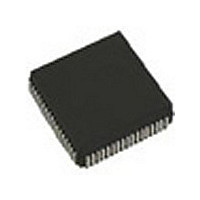
CY7C138-25JC Cypress Semiconductor Corp, CY7C138-25JC Datasheet - Page 7

CY7C138-25JC
Manufacturer Part Number
CY7C138-25JC
Description
IC SRAM 32KBIT 25NS 68PLCC
Manufacturer
Cypress Semiconductor Corp
Specifications of CY7C138-25JC
Format - Memory
RAM
Memory Type
SRAM - Dual Port, Asynchronous
Memory Size
32K (4K x 8)
Speed
25ns
Interface
Parallel
Voltage - Supply
4.5 V ~ 5.5 V
Operating Temperature
0°C ~ 70°C
Package / Case
68-PLCC
Density
32Kb
Access Time (max)
25ns
Sync/async
Asynchronous
Architecture
Not Required
Clock Freq (max)
Not RequiredMHz
Operating Supply Voltage (typ)
5V
Address Bus
12b
Package Type
PLCC
Operating Temp Range
0C to 70C
Number Of Ports
2
Supply Current
180mA
Operating Supply Voltage (min)
4.5V
Operating Supply Voltage (max)
5.5V
Operating Temperature Classification
Commercial
Mounting
Surface Mount
Pin Count
68
Word Size
8b
Number Of Words
4K
Lead Free Status / RoHS Status
Contains lead / RoHS non-compliant
Other names
428-1445
Available stocks
Company
Part Number
Manufacturer
Quantity
Price
Company:
Part Number:
CY7C138-25JC
Manufacturer:
CYPRESS
Quantity:
13 888
Company:
Part Number:
CY7C138-25JC
Manufacturer:
Cypress Semiconductor Corp
Quantity:
10 000
Switching Waveforms
Notes:
19. BUSY = HIGH for the writing port.
20. CE
21. The internal write time of the memory is defined by the overlap of CE or SEM LOW and R/W LOW. Both signals must be LOW to initiate a write, and either signal can
22. If OE is LOW during a R/W controlled write cycle, the write pulse width must be the larger of t
23. R/W must be HIGH during all address transitions.
SEM OR CE
Read Timing with Port-to-Port Delay (M/S = L)
ADDRESS
ADDRESS
Write Cycle No. 1: OE Three-States Data I/Os (Either Port)
DATA OUT
ADDRESS
terminate a write by going HIGH. The data input set-up and hold timing should be referenced to the rising edge of the signal that terminates the write.
bus for the required t
t
DATA
PWE
DATA
DATA IN
L
= CE
.
R/W
R/W
OUTL
OE
INR
R
R
R
= LOW.
L
SD
. If OE is HIGH during a R/W controlled write cycle (as in this example), this requirement does not apply and the write pulse can be as short as the specified
(continued)
t
SA
t
HZOE
[19, 20]
t
MATCH
SCE
MATCH
t
t
HIGH IMPEDANCE
AW
WC
7
t
WC
t
PWE
[21, 22, 23]
t
PWE
PWE
or (t
HZWE
t
WDD
t
t
VALID
SD
SD
DATA VALID
+ t
SD
) to allow the I/O drivers to turn off and data to be placed on the
t
DDD
t
HD
t
HD
t
LZOE
t
HA
CY7C138
CY7C139
VALID
C138-10
C138-11


